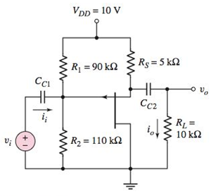
For the p−channel JFET source−follower circuit in Figure P4.78, the transistor parameters are: I D S S = 2 mA , V P = + 1.75 V , and λ = 0 . (a) Determine I D Q and V S D Q . (b) Determine the small−signal gains A υ = υ o / υ i and A i = i o / i i . (c) Determine the maximum symmetrical swing in the output voltage. Figure P4.78
For the p−channel JFET source−follower circuit in Figure P4.78, the transistor parameters are: I D S S = 2 mA , V P = + 1.75 V , and λ = 0 . (a) Determine I D Q and V S D Q . (b) Determine the small−signal gains A υ = υ o / υ i and A i = i o / i i . (c) Determine the maximum symmetrical swing in the output voltage. Figure P4.78
For the p−channel JFET source−follower circuit in Figure P4.78, the transistor parameters are:
I
D
S
S
=
2
mA
,
V
P
=
+
1.75
V
, and
λ
=
0
. (a) Determine
I
D
Q
and
V
S
D
Q
. (b) Determine the small−signal gains
A
υ
=
υ
o
/
υ
i
and
A
i
=
i
o
/
i
i
. (c) Determine the maximum symmetrical swing in the output voltage.
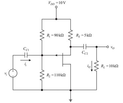
Figure P4.78
(a)
Expert Solution
To determine
The value of the IDQ and VSDQ .
Answer to Problem 4.78P
The value of the drain current IDSQ is 1mA and VSDQ is 5V .
Explanation of Solution
Given:
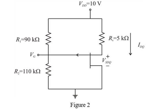
The given circuit is shown below.
Figure 1
Calculation:
The value of the voltage across the resistance R1 is given by,
VR1=90kΩ90kΩ+110kΩ(10V)=4.5V
The expression to determine the value of the voltage VR1 is given by,
VR1=VG−(5kΩ)IQ
Substitute 4.5V for VR1 in the above equation.
4.5V=VG−(5kΩ)IQIQ=4.5V−VSG5kΩ
The expression for the drain current in terms of gate to source voltage is given by,
ID=4.5V+VSG5kΩ
The expression to determine the value of the drain current is given by,
ID=IDSS(1−VGSVP)2 ….. (1)
Substitute 2mA for IDSS , 4.5V−VSG5kΩ for ID and 1.75V for VP in the above equation.
4.5V−VSG5kΩ=(2mA)(1−VGS1.75V)2VGS=0.51V
Substitute 2mA for IDSS , 0.51V for VGS and 1.75V for VP in equation (1).
ID=(2mA)(1−0.51V1.75V)2=1mA
Mark the values and redraw the circuit.
The required diagram is shown in Figure 2
The expression to determine the value of the VSDQ is given by,
VSDQ=10V−ID(5mA)
Substitute 1mA for ID in the above equation.
VSDQ=10V−(1mA)(5mA)=5V
Conclusion:
Therefore, the value of the drain current IDSQ is 1mA and VSDQ is 5V .
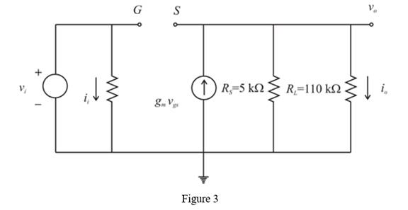
(b)
Expert Solution
To determine
The current gain and the voltage gain of the circuit.
Answer to Problem 4.78P
The value of the current gain of the circuit is 4.18 and the voltage gain is 0.844 .
Explanation of Solution
Calculation:
The expression for conductance is given by,
gm=2IDSS|VP|(1−VGSVP)
Substitute 2mA for IDSS , 1.75V for VP and 0.51V for VGS in the above equation.
gm=2(2mA)|1.75V|(1−0.51V1.75V)=1.62mA/V
The expression to determine the voltage gain is given by,
Av=gm(RS||RL)1+gm(RS||RL)
Substitute 1.62mA/V for
gm , 5kΩ for RL and 10kΩ for RS in the above equation.
Using a positive Clamper Circuit, with an AC voltage of Vi = 100v with a frequency of 30hz, a value of 1000u for the Capacitor, a silicon
diode and a resistor with the value of 100 ohms. Find the voltage value on the resistor at a simulation of Oms.
Vm
2Vm
Vo
-Vm
Input Waveform
Output Waveform
Positive Clamper circuit
Q4)
Determine and sketch the output voltage across the load resistor (RL) for the circuit shown below
(assume Si diodes)
V_DC
V DC
0,75
(1+
0.25
V_SIN
V SIN
RL
-1
V SOR
V_SQR
0.75
-0.75
V TRI
1
V_TRI
-1
Using a positive Clamper Circuit, with an AC voltage of Vi = 13v with a frequency of 60hz, a value of 100u for the Capacitor, a silicon
diode and a resistor with the value of 1000 ohms. Find the voltage value on the resistor at a simulation of 20ms.
2Vm
Vm
Vm
Vo
-Vm
Input Waveform
Output Waveform
Positive Clamper circuit
Need a deep-dive on the concept behind this application? Look no further. Learn more about this topic, electrical-engineering and related others by exploring similar questions and additional content below.


 Introductory Circuit Analysis (13th Edition)Electrical EngineeringISBN:9780133923605Author:Robert L. BoylestadPublisher:PEARSON
 Delmar's Standard Textbook Of ElectricityElectrical EngineeringISBN:9781337900348Author:Stephen L. HermanPublisher:Cengage Learning
 Programmable Logic ControllersElectrical EngineeringISBN:9780073373843Author:Frank D. PetruzellaPublisher:McGraw-Hill Education
 Fundamentals of Electric CircuitsElectrical EngineeringISBN:9780078028229Author:Charles K Alexander, Matthew SadikuPublisher:McGraw-Hill Education
 Electric Circuits. (11th Edition)Electrical EngineeringISBN:9780134746968Author:James W. Nilsson, Susan RiedelPublisher:PEARSON
 Engineering ElectromagneticsElectrical EngineeringISBN:9780078028151Author:Hayt, William H. (william Hart), Jr, BUCK, John A.Publisher:Mcgraw-hill Education,