
Videos
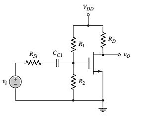
Consider the circuit shown in Figure 4.14. Assume transistor parameters of
The design parameters of the circuit. The small-signal voltage gain.
Answer to Problem 4.4EP
Design parameters are:
Small-signal voltage gain is
Explanation of Solution
Given Information:
The given circuit diagram is shown below.
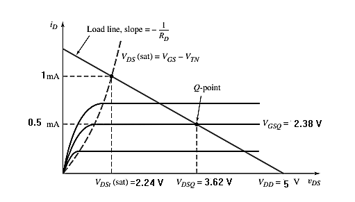
The Q -point is in the center of the saturation region.
Calculation:
If the Q -point is to be in the middle of saturation region, the current at the transition point must be
Calculating
If the Q -point is to be in the middle of saturation region, the value of
It would yield a 2.76 V peak to peak symmetrical output voltage.
The value of
The value of
The figure of load line is:
The value of
The value of
The value of transconductance is:
The small-signal output resistance is:
The small-signal equivalent circuit is:
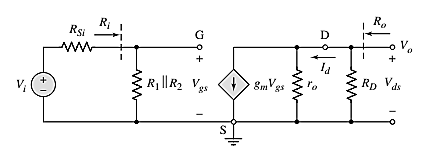
The output voltage is:
The value of
Applying voltage division rule:
Putting the value of
The value of small signal voltage gain is:
Want to see more full solutions like this?
Chapter 4 Solutions
Microelectronics: Circuit Analysis and Design


- 8 UTM Figure B.1 shows a diode circuit and its DC load line analysis. Based on the SUT information obtained UT UT I kQ + VpQ- 3 UTM UTM Vs 3 500 2 UTM & UM TM &UTM UTM UTM &UTM 5 UTM Figure B.1 UTM & U UTM VD (V) 0.72 UTM i UTM UTMarrow_forwardBriefly describe the operation of a silicon n-channel JFET, including effect of the gate voltages VG = 0 and VG < 0 and source-drain voltages Vos on the flow of charge carriers in the device before and after 'pinch-off'. Use an l-V graph to illustrate your answer. 4. Gate Source Drain FIGURE CREDIT: An Introduction to Semiconductor Devices, D. Neamenarrow_forward2. In the emitter follower discussed in the lectures, the output (emitter) voltage is 0.7V below the input (base) voltage. One way to remove this offset is to use a diode as shown below left. Suppose our input Vi=2V. Assume beta = 100, VCE,SAT=0V, VBE,ON=0.7, and diode VF=0.7. +5V +5V 1000 R1 1N4148 500 100 Scattering Limit Vo 10 Vi o RL=10 R2 T, = 25 °C 0.1 1K 0 0.4 0.8 1.2 1.6 2.0 V, - Forward Voltage (V) 94 9170 a. Determine VB and V. b. Verify your assumed state of the BJT from (a) c. Verify your assumed state of the diode from (a) d. (Optional challenge) To provide good matching between the diode VF and VBE,ON, we need to have at least 1mA passing through ID, as shown in the datasheet figure above right. What is the maximum V; for which Ip is at least 1mA? To increase this limit, should we change R1 or R2 and in what direction (increase or decrease)? -Forward Current (mA)arrow_forward
- A pn Junction is fabricated on top of a Si substrate. At 300 K, the donor and acceptor doping densities are ND= 3x10¹⁸/cm3 and NA=2.5x10¹⁵/cm3. If the pn junction is in unbiased condition, then what will be the thickness of the depletion region?arrow_forwardWhich of the following is a type of Metal Oxide Semiconductor Field Effect Transistor: O P channel JFET O None of them O N channel D- MOSFET in O N channel JFET A simple diode rectifier has 'ripples in the output wave which makes it unsuitable as a DC source. To overcome this one can use of a capacitor in series with a the load resistance. stion Select one: O True O Falsearrow_forward2. In the emitter follower discussed in the lectures, the output (emitter) voltage is 0.7V below the input (base) voltage. One way to remove this offset is to use a diode as shown below left. Suppose our input Vi=2V. Assume beta = 100, VCE,SAT=OV, VBE,ON=0.7, and diode Vş=0.7. +5V +5V 1000 R, 500 1N4148 100 Scattering Limit Vo 10 Vio RL=10 R2 -T,= 25 °C 0.1 1K 0.4 0.8 1.2 1.6 2.0 V, - Forward Voltage (V) 94 9170 a. Determine VB and Vo b. Verify your assumed state of the BJT from (a) c. Verify your assumed state of the diode from (a) d. (Optional challenge) To provide good matching between the diode V; and VBE,ON, we need to have at least 1ma passing through Io, as shown in the datasheet figure above right. What is the maximum V, for which Ip is at least 1mA? To increase this limit, should we change R1 or R2 and in what direction (increase or decrease)? 1,- Forward Current (mA)arrow_forward
- What happens to the depletion width as we increase the doping level on both sides of a p-n junction? Explain conceptuallyarrow_forwardWhat is the output voltage across a load resistor if it is paralleled with a forward biased silicon diode? The resistor network is supplied with 10 V. * O A. 0.7 V O B. 9.3 V O C. 10 V O D. Can't be solve, lack of data.arrow_forward" A 2N5459 has VGS(off) = -8 v and IDSS = %3D 16mA. What is the drain current at the half cutoff point?arrow_forward
- Q.3 The input, Vs and the output, Vo of a diode circuit (assuming ideal diode) are shown 3 SEEU/SKEU 1063 in Figure A.2. Name an application that can produce output as in Figure A.2 (ii) and draw the circuit. S UTM S UTM UTM UTM S UTM S UTM O UTM 8 UTM UTM S UTM S UTM UTM UTM S UTM UTM MB UTM ot UTM UT S UTM B UTM UTM 8UTM (i) aUTM UT 8 UTM UTM UTM M UTM TM S UTM UTM UT MS UTM or (i) UTM Figure A.2 8 UTM UT TM S UTMarrow_forwardGiven the circuit design for a Zener diode regulator in the previous question, what is the maximum power that will be dissipated by the Rs resistor? You are told that the source voltage Vs varies from 6 V to 11 V, the load current il varies between 2 mA and 45 mA, and the diode is an ideal 3 V Zener diode. You will need to recalculate the maximum allowable resistance Rs with your new values, as part of this question. Please enter your answer to 3 significant figures, and in Watts.arrow_forwardIRL RL In the circuit using a Zener diode above, given that V, = 10 V, R= 3.7 KO, R 6.8 KQ, and the Zener voltage Vz = 5 V. a) The current IRL through the load resistor is b) The current fiowing through the resistor R is:arrow_forward
 Introductory Circuit Analysis (13th Edition)Electrical EngineeringISBN:9780133923605Author:Robert L. BoylestadPublisher:PEARSON
 Delmar's Standard Textbook Of ElectricityElectrical EngineeringISBN:9781337900348Author:Stephen L. HermanPublisher:Cengage Learning
 Programmable Logic ControllersElectrical EngineeringISBN:9780073373843Author:Frank D. PetruzellaPublisher:McGraw-Hill Education
 Fundamentals of Electric CircuitsElectrical EngineeringISBN:9780078028229Author:Charles K Alexander, Matthew SadikuPublisher:McGraw-Hill Education
 Electric Circuits. (11th Edition)Electrical EngineeringISBN:9780134746968Author:James W. Nilsson, Susan RiedelPublisher:PEARSON
 Engineering ElectromagneticsElectrical EngineeringISBN:9780078028151Author:Hayt, William H. (william Hart), Jr, BUCK, John A.Publisher:Mcgraw-hill Education,