
Microelectronics: Circuit Analysis and Design
4th Edition
ISBN: 9780073380643
Author: Donald A. Neamen
Publisher: McGraw-Hill Companies, The
expand_more
expand_more
format_list_bulleted
Concept explainers
Videos
Textbook Question
Chapter 1, Problem 1.40P
The diode in the circuit shown in Figure P1.40 has a reverse−saturation current of
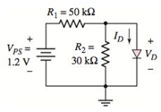
Figure P1.40
Expert Solution & Answer
Want to see the full answer?
Check out a sample textbook solution
Students have asked these similar questions
In the circuit given in the figure, find the current passing through the diode in mA since R1 = 4.95Kohm, R2 = 2.50Kohm, R3 = 1.69Kohm, R4 = 5.44Kohm, VCC = 13.00V and the diode is silicon?
0:- Consider the circuit in Figure
a) What type of circuit is this?
b) Find and Sketch the voltage
waveform across RL, assume
the diodes are practical.
c) If 100uf
capacitor
parallel with the
resistor, calculate the ripple
is
connected
factor
I O o D
(c)
Reverse recovery is a common problem in a diode. It can increase switching losses,
increase forward voltage and induce voltage surge.
(i)
Explain how reverse recovery can increase switching losses in a diode.
(ii)
Figure Q1(c) shows that characteristic of reverse recovery in a diode. Based on
the figure, calculate the peak reverse recovery current I,
I (A)
dls
dt
30 A
Q,,
1 us
3 us
Figure Q1(c): The characteristic of reverse recovery in a diode
Chapter 1 Solutions
Microelectronics: Circuit Analysis and Design
Ch. 1 - Calculate the intrinsic carrier concentration in...Ch. 1 - (a) Calculate the majority and minority carrier...Ch. 1 - Consider ntype GaAs at T=300K doped to a...Ch. 1 - Consider silicon at T=300K . Assume the hole...Ch. 1 - Determine the intrinsic carrier concentration in...Ch. 1 - (a) Consider silicon at T=300K . Assume that...Ch. 1 - Using the results of TYU1.2, determine the drift...Ch. 1 - The electron and hole diffusion coefficients in...Ch. 1 - A sample of silicon at T=300K is doped to...Ch. 1 - (a) Calculate Vbi for a GaAs pn junction at T=300K...
Ch. 1 - A silicon pn junction at T=300K is doped at...Ch. 1 - (a) A silicon pn junction at T=300K has a...Ch. 1 - (a) Determine Vbi for a silicon pn junction at...Ch. 1 - A silicon pn junction diode at T=300K has a...Ch. 1 - Recall that the forwardbias diode voltage...Ch. 1 - Consider the circuit in Figure 1.28. Let VPS=4V ,...Ch. 1 - (a) Consider the circuit shown in Figure 1.28. Let...Ch. 1 - The resistor parameter in the circuit shown in...Ch. 1 - Consider the diode and circuit in Exercise EX 1.8....Ch. 1 - Consider the circuit in Figure 1.28. Let R=4k and...Ch. 1 - The power supply (input) voltage in the circuit of...Ch. 1 - (a) The circuit and diode parameters for the...Ch. 1 - Determine the diffusion conductance of a pn...Ch. 1 - Determine the smallsignal diffusion resistance of...Ch. 1 - The diffusion resistance of a pn junction diode at...Ch. 1 - A pn junction diode and a Schottky diode both have...Ch. 1 - Consider the circuit shown in Figure 1.45....Ch. 1 - Consider the circuit shown in Figure 1.46. The...Ch. 1 - A Zener diode has an equivalent series resistance...Ch. 1 - The resistor in the circuit shown in Figure 1.45...Ch. 1 - Describe an intrinsic semiconductor material. What...Ch. 1 - Describe the concept of an electron and a hole as...Ch. 1 - Describe an extrinsic semiconductor material. What...Ch. 1 - Describe the concepts of drift current and...Ch. 1 - How is a pn junction formed? What is meant by a...Ch. 1 - How is a junction capacitance created in a...Ch. 1 - Write the ideal diode currentvoltage relationship....Ch. 1 - Describe the iteration method of analysis and when...Ch. 1 - Describe the piecewise linear model of a diode and...Ch. 1 - Define a load line in a simple diode circuit.Ch. 1 - Under what conditions is the smallsignal model of...Ch. 1 - Describe the operation of a simple solar cell...Ch. 1 - How do the i characteristics of a Schottky barrier...Ch. 1 - What characteristic of a Zener diode is used in...Ch. 1 - Describe the characteristics of a photodiode and a...Ch. 1 - (a) Calculate the intrinsic carrier concentration...Ch. 1 - (a) The intrinsic carrier concentration in silicon...Ch. 1 - Calculate the intrinsic carrier concentration in...Ch. 1 - (a) Find the concentration of electrons and holes...Ch. 1 - Gallium arsenide is doped with acceptor impurity...Ch. 1 - Silicon is doped with 51016 arsenic atoms/cm3 ....Ch. 1 - (a) Calculate the concentration of electrons and...Ch. 1 - A silicon sample is fabricated such that the hole...Ch. 1 - The electron concentration in silicon at T=300K is...Ch. 1 - (a) A silicon semiconductor material is to be...Ch. 1 - (a) The applied electric field in ptype silicon is...Ch. 1 - A drift current density of 120A/cm2 is established...Ch. 1 - An ntype silicon material has a resistivity of...Ch. 1 - (a) The applied conductivity of a silicon material...Ch. 1 - In GaAs, the mobilities are n=8500cm2/Vs and...Ch. 1 - The electron and hole concentrations in a sample...Ch. 1 - The hole concentration in silicon is given by...Ch. 1 - GaAs is doped to Na=1017cm3 . (a) Calculate no and...Ch. 1 - (a) Determine the builtin potential barrier Vbi in...Ch. 1 - Consider a silicon pn junction. The nregion is...Ch. 1 - The donor concentration in the nregion of a...Ch. 1 - Consider a uniformly doped GaAs pn junction with...Ch. 1 - The zerobiased junction capacitance of a silicon...Ch. 1 - The zerobias capacitance of a silicon pn junction...Ch. 1 - The doping concentrations in a silicon pn junction...Ch. 1 - (a) At what reversebias voltage does the...Ch. 1 - (a) The reversesaturation current of a pn junction...Ch. 1 - (a) The reversesaturation current of a pn junction...Ch. 1 - A silicon pn junction diode has an emission...Ch. 1 - Plot log10ID versus VD over the range 0.1VD0.7V...Ch. 1 - (a) Consider a silicon pn junction diode operating...Ch. 1 - A pn junction diode has IS=2nA . (a) Determine the...Ch. 1 - The reversebias saturation current for a set of...Ch. 1 - A germanium pn junction has a diode current of...Ch. 1 - (a)The reversesaturation current of a gallium...Ch. 1 - The reversesaturation current of a silicon pn...Ch. 1 - A silicon pn junction diode has an applied...Ch. 1 - A pn junction diode is in series with a 1M...Ch. 1 - Consider the diode circuit shown in Figure P1.39....Ch. 1 - The diode in the circuit shown in Figure P1.40 has...Ch. 1 - Prob. 1.41PCh. 1 - (a) The reversesaturation current of each diode in...Ch. 1 - (a) Consider the circuit shown in Figure P1.40....Ch. 1 - Consider the circuit shown in Figure P1.44....Ch. 1 - The cutin voltage of the diode shown in the...Ch. 1 - Find I and VO in each circuit shown in Figure...Ch. 1 - Repeat Problem 1.47 if the reversesaturation...Ch. 1 - (a) In the circuit Shown in Figure P1.49, find the...Ch. 1 - Assume each diode in the circuit shown in Figure...Ch. 1 - (a) Consider a pn junction diode biased at IDQ=1mA...Ch. 1 - Determine the smallsignal diffusion resistancefor...Ch. 1 - The diode in the circuit shown in Figure P1.53 is...Ch. 1 - The forwardbias currents in a pn junction diode...Ch. 1 - A pn junction diode and a Schottky diode have...Ch. 1 - The reversesaturation currents of a Schottky diode...Ch. 1 - Consider the Zener diode circuit shown in Figure...Ch. 1 - (a) The Zener diode in Figure P1.57 is ideal with...Ch. 1 - Consider the Zener diode circuit shown in Figure...Ch. 1 - The Output current of a pn junction diode used as...Ch. 1 - Using the currentvoltage characteristics of the...Ch. 1 - (a) Using the currentvoltage characteristics of...Ch. 1 - Use a computer simulation to generate the ideal...Ch. 1 - Use a computer simulation to find the diode...Ch. 1 - Design a diode circuit to produce the load line...Ch. 1 - Design a circuit to produce the characteristics...Ch. 1 - Design a circuit to produce the characteristics...Ch. 1 - Design a circuit to produce the characteristics...
Knowledge Booster


Learn more about
Need a deep-dive on the concept behind this application? Look no further. Learn more about this topic, electrical-engineering and related others by exploring similar questions and additional content below.Similar questions
- How is a solid-state diode tested? Explain.arrow_forwardConsider the circuit in the figure below 4:1 120 V rms ooooo gll reelee D₁ L a. What type of circuit is this? b. What is the total peak secondary voltage? D₂ c. Find the peak voltage across each half of the secondary. d. Sketch the voltage waveform across RL. e. What is the peak current through each diode? f. What is the PIV for each diode? RL 1.0 ΚΩarrow_forwardA zener diode exhibits a certain change in VZ for a certain change in IZ on a portion of the linear characteristic curve between IZK and IZM as illustrated in Figure 5. Calculate the zener impedance.arrow_forward
- Draw vx and v0 according to the input voltages in the circuit shown in the figure. note = R1 = 10Kohm R2 = 1kohm R3 = 1Kohm, the threshold voltages of diodes will be VE = 0.7V.arrow_forwardDetermine the negative resistance for the tunnel diode in the figure between ?T = 0.2 ? and ?T = 0.4arrow_forwardConsider a Zener diode in the figure given below where, V1 = 30 V. Determine the Zener current IZ if RZ = 100 Ω.arrow_forward
- For the circuit below, assume the diodes operate with a constant voltage drop of .7V, find Vx, Vy, VD4 and ID2. 15V 15V Allt V1 V2 R1 1k IDC 1mA Vx R2 2k ww D1N4002 Vy D1N4002 7D1 D1N4002 D2 D3 R3 1k D4 D1N4002arrow_forwardGiven the circuits below, Use ideal diode. a. what is the charge voltage across the capacitor in figure a? b. what is the stable voltage range at the output of figure a? + + C R 10 V + Vi 20vpeak ā 19arrow_forwardJunction Diode Give the following details of the diode: Schematic symbol Construction Characteristic Curve Basic operation (including mathematical equation if there's any) Applicationsarrow_forward
- uO 9:.0 A docs.google.com * ZAIN IQ l. Q3/B: Assume an ideal diode model for all the diodes in the circuit below. calculate voltages and currents through D1 and D2 9kQ 1N1199C R2 D1 18KQ 1N1199C D3 1N1199C V2 =12 V R3 1kQ R4 5kQ 1.22 V 11 mA 0.5 A O VD1 ID1 VD2 ID2 صفحة 4 من 6arrow_forward1. Half-wave battery charger. Consider the battery charging circuit in Figure. with Vm= 20V, R= 10Nand VB= 14V. Find the peak current assuming an ideal diode. Current limiting resistor R + Vsin(@x) i(t) VBarrow_forwardIn the circuit shown in the figure; B) When RL = 1Kohm and capacitor C is deactivated, draw VA and V0 in scale according to input voltage Vs. NOTE = diodes are idealarrow_forward
arrow_back_ios
SEE MORE QUESTIONS
arrow_forward_ios
Recommended textbooks for you

Diodes Explained - The basics how diodes work working principle pn junction; Author: The Engineering Mindset;https://www.youtube.com/watch?v=Fwj_d3uO5g8;License: Standard Youtube License