Logic gate:
- Logic gate is an electronic circuit that is used to take logical decisions based on the input.
- It contains one or more number of inputs and one output.
- The working of logic gate is based on the binary principle that has two states either logic 0 or logic 1.
- The output of logic gate is produced when it satisfies any of its logic conditions.
- The logic condition depends upon the type of the gates and the number of inputs.
- The primary logic gates include AND, OR and NOT and the combinations of these gates are used to implement any of the other logic gates.
AND gate:
- The AND gate refers to a logic gate whose output will be HIGH only when all the inputs are HIGH.
- The output of AND gate will be LOW when any one of its input is LOW.
- The symbol to represent AND gate is given below:
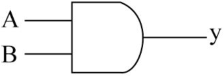
- The truth table for AND gate is as follows:
| INPUT A | INPUT B | OUTPUT Y |
| 0 | 0 | 0 |
| 0 | 1 | 0 |
| 1 | 0 | 0 |
| 1 | 1 | 1 |
OR gate:
- The OR gate refers to a logic gate whose output will be HIGH when any one of its inputs are HIGH.
- The output of AND gate will be LOW when both the inputs are LOW.
- The symbol to represent OR gate is given below:
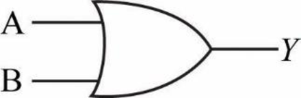
- The truth table for OR gate is as follows:
| INPUT A | INPUT B | OUTPUT Y |
| 0 | 0 | 0 |
| 0 | 1 | 1 |
| 1 | 0 | 1 |
| 1 | 1 | 1 |
NOT gate:
- The NOT gate refers to a logic gate whose output will be HIGH when it’s input is LOW and whose output will be LOW when it’s input is HIGH.
- The symbol to represent NOT gate is given below:
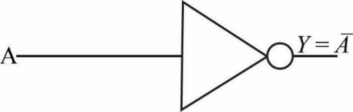
- The truth table for NOT gate is as follows:
| INPUT A | OUTPUT Y |
| 0 | 1 |
| 1 | 0 |
Explanation of Solution
b.
Logic gate circuit:
The logic gate circuit for the given Boolean expression
Explanation:
In the above given logic gate circuit,
- The inputs “A” and “B” are connected to logic AND gate and the corresponding output will be (AB)
Explanation of Solution
c.
Logic gate circuit:
The logic gate circuit for the given Boolean expression
Explanation:
In the above given logic gate circuit,
- The inputs “A” and “B” are connected to logic OR gate and the corresponding output will be (A+B).
- The input “C” is connected to logic NOT gate and the corresponding output will be “
Explanation of Solution
d.
Logic gate circuit:
The logic gate circuit for the given Boolean expression
Explanation:
In the above given logic gate circuit,
- The inputs “C” and “D” are connected to logic AND gate and the corresponding output will be (CD).
- Now, the resultant along with other input “B” is connected to logic OR gate whose output will be
Explanation of Solution
e.
Logic gate circuit:
The logic gate circuit for the given Boolean expression
Explanation:
In the above given logic gate circuit,
- The input “A” is connected to logic NOT gate and the corresponding output will be “
Explanation of Solution
f.
Logic gate circuit:
The logic gate circuit for the given Boolean expression
Explanation:
In the above given logic gate circuit,
- The inputs “A”, “B” and “C” are connected to logic AND gate and the corresponding output will be (ABC).
- Now, the resultant along with the other input “D” is connected to logic OR gate whose output will be

Trending nowThis is a popular solution!

Chapter 4 Solutions
Programmable Logic Controllers

- Consider the following logic circuit. A B Do - F a) Write the Boolean function F(A, B, C). b) Simplify the function using Boolean algebra. c) Draw an equivalent circuit with only two gates. d) Draw the truth table of F.arrow_forwardDraw a logic circuit that performed by this logic expression: * Ā·(Ē + C) · Ď · E = Yarrow_forwardTask 4: Simplifying Boolean functions Simplify the following Boolean expression F (A, B, C) = (A+C") +C (C.A' + (B.A) +C Draw the simplified Boolean expression using EWB. Find out the truth table of the circuit.arrow_forward
- 2. Write the Boolean expression of the given logic circuit as shown below. X. F =arrow_forwardDraw the logic circuit represented by each of the following expressions: . AB + AB ( ● • AB(CD + EF)arrow_forwardQ5// Design a combinational .logic circuit that has 4-inputs (A,B,C,D) and one-output (F), the output will be high "1" when the majority of inputs are high"1", and then simplify the output use POS expression in K-map and draw logic circuit.arrow_forward
- Part a Design a logic circuit using the truth table Inputs output shown. Use only basic logic gates (AND, OR, NOT). Also, the circuit should use the FEWEST number of gates and the FEWEST number of inputs to the gates. Fully label all the inputs and outputs. a b. 1 1 1 1 1. 1 1 Part b Implement a 3-input XOR gate using only a 4x1 multiplexer and an inverter. Also complete the truth table in your answer sheets with the correct labels and function solution. Fully label all inputs and outputs. Part c Design a full-adder using half-adders and A- additional logic using the half-adder shown here. Pi Giarrow_forward* A combinational circuit has 3 inputs X, Y, Z and output F. F is 1 for following input combinations: X is 0, Y is 1. X is 0, Z is 1. X, Y, Z are 0. X, Y, Z are 1. Otherwise F is 0 а) Write the truth table of the function b) Find the minimum product-of-sums equation с) Draw logic circuit using minimum number of 2-input NAND gatesarrow_forwardSimplify the boolean expression B (x, y, z) = X’Z+X’Y+YZarrow_forward
- Q4 Draw logic gates for the function F. F (A, B, C, D) = (B'D) (A'+ C°D) + (BC'+ D'A)arrow_forward2. Consider the circuit below. a. Write the Boolean expression for output F in terms of A, B and C. b. Construct a truth table for the circuit with A as MSB and C as LSB. c. Write the Canonical SOP and POS forms for output F. A B C 3. Draw the logic circuit represented by the expression F(A, B) = AB using no more than 5 units of 2-input NAND gate and write the corresponding Boolean expression.arrow_forward1. A combinational circuit is specified by the three Boolean functions: F(A, B, C) = C(A' + B') + AC' + BC' G(A, B, C) = ABC + BC H(A, B, C) = A + B a. b. C. Create a truth table for the circuit. Simplify the expressions using Karnaugh maps. Draw the logic diagram for the circuit using the simplified expressions obtained in part b.arrow_forward
 Database System ConceptsComputer ScienceISBN:9780078022159Author:Abraham Silberschatz Professor, Henry F. Korth, S. SudarshanPublisher:McGraw-Hill Education
 Starting Out with Python (4th Edition)Computer ScienceISBN:9780134444321Author:Tony GaddisPublisher:PEARSON
 Digital Fundamentals (11th Edition)Computer ScienceISBN:9780132737968Author:Thomas L. FloydPublisher:PEARSON
 C How to Program (8th Edition)Computer ScienceISBN:9780133976892Author:Paul J. Deitel, Harvey DeitelPublisher:PEARSON
 Database Systems: Design, Implementation, & Manag...Computer ScienceISBN:9781337627900Author:Carlos Coronel, Steven MorrisPublisher:Cengage Learning
 Programmable Logic ControllersComputer ScienceISBN:9780073373843Author:Frank D. PetruzellaPublisher:McGraw-Hill Education