Practical Management Science
6th Edition
ISBN: 9781337406659
Author: WINSTON, Wayne L.
Publisher: Cengage,
expand_more
expand_more
format_list_bulleted
Concept explainers
Question
thumb_up100%
Chapter 3, Problem 1C
Summary Introduction
Case summary:
The case discusses the details about the Company SS, which would manufacture two types of shelves for the grocery stores. The essential details are given below:
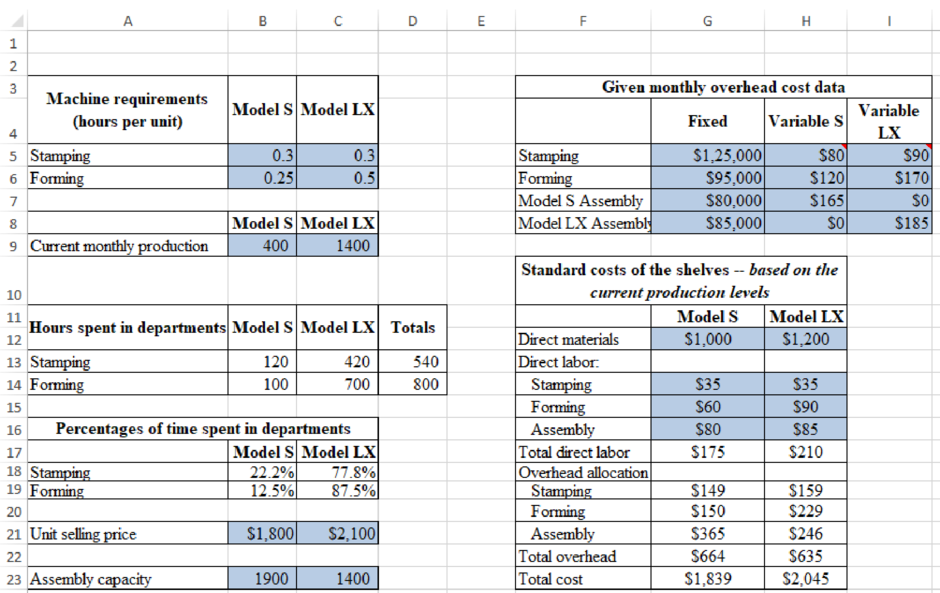
Figure (1)
To determine: The LP model of the problem.
Expert Solution & Answer

Trending nowThis is a popular solution!

Students have asked these similar questions
JCL Inc. is a major chip manufacturing firm that sells its products to computer manufacturers like Dell, HP, and others. In simplified terms, chip making at JCL Inc. involves three basic operations: depositing, patterning, and etching.
Depositing: Using chemical vapor deposition (CVD) technology, an insulating material is deposited on the wafer surface, forming a thin layer of solid material on the chip.
Patterning: Photolithography projects a microscopic circuit pattern on the wafer surface, which has a light-sensitive chemical like the emulsion on photographic film. It is repeated many times as each layer of the chip is built.
Etching: Etching removes selected material from the chip surface to create the device structures.
The following table lists the required processing times and setup times at each of the steps. Assume that the unit of production is a wafer, from which individual chips are cut at a later stage.
Note: A setup can only begin once the batch has arrived at the…
A manufacturing cell makes three models of a product – AKC1011, BC0001, and AC0102. The daily demand for the three products are as follows: 200 of AKC1011, 500 BC0001, and 300 of AC0102. Develop a balanced mixed-model sequence that should be repeated throughout the day in order to meet demand.
JCL Inc. is a major chip manufacturing firm that sells its products to computer manufacturers like Dell, Gateway, and others. In simplified terms, chip making at JCL Inc. involves three basic operations: depositing, patterning, and etching.
Depositing: Using chemical vapor deposition (CVD) technology, an insulating material is deposited on the wafer surface, forming a thin layer of solid material on the chip.
Patterning: Photolithography projects a microscopic circuit pattern on the wafer surface, which has a light-sensitive chemical like the emulsion on photographic film. It is repeated many times as each layer of the chip is built.
Etching: Etching removes selected material from the chip surface to create the device structures.
The table below lists the required processing times and setup times at each of the steps. There is unlimited space for buffer inventory between these steps. Assume that the unit of production is a wafer, from which individual chips are cut at a later…
Chapter 3 Solutions
Practical Management Science
Ch. 3.6 - Prob. 1PCh. 3.6 - Prob. 2PCh. 3.6 - Prob. 3PCh. 3.6 - Prob. 4PCh. 3.6 - Prob. 5PCh. 3.6 - Prob. 6PCh. 3.6 - Prob. 7PCh. 3.6 - Prob. 8PCh. 3.6 - Prob. 9PCh. 3.7 - Prob. 10P
Ch. 3.7 - Prob. 11PCh. 3.7 - Prob. 12PCh. 3.7 - Prob. 13PCh. 3.7 - Prob. 14PCh. 3.7 - Prob. 15PCh. 3.7 - Prob. 16PCh. 3.7 - Prob. 17PCh. 3.8 - The Pigskin Company produces footballs. Pigskin...Ch. 3.8 - The Pigskin Company produces footballs. Pigskin...Ch. 3.8 - The Pigskin Company produces footballs. Pigskin...Ch. 3.8 - Prob. 21PCh. 3.8 - Prob. 22PCh. 3.8 - Prob. 23PCh. 3.8 - Prob. 24PCh. 3 - Prob. 25PCh. 3 - Prob. 26PCh. 3 - Prob. 27PCh. 3 - Prob. 28PCh. 3 - Prob. 29PCh. 3 - Prob. 30PCh. 3 - Prob. 31PCh. 3 - Prob. 32PCh. 3 - Prob. 33PCh. 3 - Prob. 34PCh. 3 - Prob. 35PCh. 3 - Prob. 36PCh. 3 - Prob. 37PCh. 3 - Prob. 38PCh. 3 - Prob. 39PCh. 3 - Prob. 40PCh. 3 - Prob. 41PCh. 3 - Prob. 42PCh. 3 - Prob. 43PCh. 3 - Prob. 44PCh. 3 - Prob. 45PCh. 3 - Prob. 46PCh. 3 - Prob. 47PCh. 3 - Prob. 48PCh. 3 - Prob. 49PCh. 3 - Prob. 50PCh. 3 - Prob. 51PCh. 3 - Prob. 52PCh. 3 - Prob. 1C
Knowledge Booster


Learn more about
Need a deep-dive on the concept behind this application? Look no further. Learn more about this topic, operations-management and related others by exploring similar questions and additional content below.Similar questions
- Will’s Welded Widgets (WWW) makes its Q Model from components R, S, and T. Component R is made from 2 units of component X and 2 unit of component Y. Component T is made from 1 unit of component V and 2 units of component Z. Calculate the gross requirements for each of the components when the company plans to build 70 of its Q Model if you have these inventories: 70 units of component T and 110 units of component R, using the given information: Item Usage per Parent Q - R 2 S 2 T 1 X 2 Y 2 V 1 Z 2 Q R S T X Y V Z Put the answers down into the table: (If answer is zero, please enter 0, do not leave any fields blank.) Product Gross Requirements Q…arrow_forwardYou are the president of XYZ Manufacturing company. You have recently learned about the following issue: A month ago, the company’s general manager (GM) told one of the line managers to produce an extra 15,000 units of a product so that there would be inventory in stock for the next time the item is ordered. Last week, the GM scolded the line manager for having 15,000 units of the item in stock. The GM told the line manager that producing excess inventory costs the company money and should never be done. The GM then puts the line manager on a performance plan. This is not the first time you have heard about the GM telling an employee to do one thing only to criticize him or her for doing it later. This employee feels very frustrated by this, but does not want to make a formal complaint because she has seen other employees lose their jobs or get demoted for questioning the GM. Create an outline that proposes a leadership solution to this issue. The outline should address the following:…arrow_forwardA company wants to store the following seven SKUs so there is 100% accessibility.Items are stored on pallets that are stored four high.a. How many pallet positions are needed?b. What is the cube utilization? c. If the company bought racking for storing the pallets, how many pallet positionsare needed to give 100% accessibility?arrow_forward
- A manufacturer of Blu-ray Discs (BDs) estimates the yearly demand for a BD to be 10,000. It costs $400 to set up the machinery to burn the BDs, plus $3 for each one produced. If it costs the company $2 to store a BD for a year, how many should be burned at a time and how many production runs will be needed to minimize costs? BDs burned at a time production runsarrow_forwardA company wishes to store the following SKUs so there is 100% accessibility. Theitems are stored on pallets that can be stacked three high.a. How many pallet positions are needed?b. What is the cube utilization?c. If the company bought racking for storing the pallets, how many pallet positionsare needed to give 100% accessibility?arrow_forwardReduces costs and their feasibility ranges are rooted in making changes in the right hand side of the constraint. Your answer: True Falsearrow_forward
- A manufacturer has a production facility that requires 10,237 units of component JY21 per year. Following a long-term contract, the manufacturer purchases component JY21 from a supplier with a lead time of 6 days. The unit purchase cost is $31.4 per unit. The cost to place and process an order from the supplier is $168 per order. The unit inventory carrying cost per year is 12.2 percent of the unit purchase cost. The manufacturer operates 250 days a year. Assume EOQ model is appropriate. If the manufacturer uses a constant order quantity of 1,053 units per order, what is the annual holding cost? Use at least 4 decimal places.arrow_forwardList the system of inequalities which describe B in the graph below.ECON1003 Mathematics for Social Sciences Unit 3_Version 1 Page 33 6. Anya’s Jeans has production process organized in threedistinct stages: cutting; sewing and finishing. She produces threetypes of jeans, namely peddle-pushers, hipsters and low cuts. Thenumber of minutes each type requires in each production processin shown below.Type Cutting Sewing FinishingPeddle-Pusher 4 6 2Hipster 6 7 4Low Rider 9 3 6On average, there are 6400 minutes of cutting time, 3500 minutes ofsewing time and 2400 minutes of finishing time each day. Given thatthe company makes $10 profit on each peddle-pusher $ 50 on eachhipster and $60 on each low cut and that the company sells all thejeans made. List the system of inequalities for the cutting, sewingand finishing constraints.arrow_forwardIn a large microelectronics plant, the assembly cell for circuit boards has a demand for 300 units an hour. Two feeder cells supply partsA and B to the assembly cell (one A and one B for each board). Standard containers that look like divided trays are used. A container will hold 22 As or 13 Bs. It takes 13 minutes to fill up a container with As and 22 minutes to fill up a container with Bs. Transit time to the assembly cell is 5 minutes for both A and B. No safety factor is used. Kanbans to be circulated Between Process A and Assembly cell? Kanbans to be circulated Between Process B and Assembly cell?arrow_forward
- Suppose Firm A can manufacture 100 pens and 20 umbrellas with a unit of labor, and Firm B can manufacture 80 pens and 10 umbrellas with a unit of labor. Which one of the following statements is true? Firm A has the comparative advantage in both pen and umbrella production.Firm B has an absolute advantage in umbrella production.Firm A has a comparative advantage only in pen production.Firm B has a comparative advantage in pen production.Neither firm has a comparative advantage in either pen or umbrella production.arrow_forwardA plastic canister manufacturing company maintains an annual safety stock of 500 units of plastic caps. If the company places an annual purchase order for 1,800 units of these caps, its average annual inventory, in units, is between: ( )1,500 and 1,300 ( )3,200 and 3,000 ( )2,400 and 2,200 ( )1,200 and 1,000 ( )1,900 and 1,700arrow_forwardHansen Controls has been awarded a contract for a large number of control panels. To meet this demand, it will use its existing plants in Houston and Tulsa, and consider new plants in Portland, St. Louis and Lexington. Finished control panels are to be shipped to Denver, Kansas City and Seattle. Pertinent information is given in the table. Denver 1 1- 2- 3- Sources 4- 5- Houston Tulsa Portland Construction St. Louis Cost Kansas City 2 ---- 1 Shipping Cost to Destination: Capacity Seattle 3 6 6 500,000 450,000 Lexington 400,000 Demand 14,000 13,000 18,000 We develop a transportation model as an LP that includes provisions for the fixed costs (construction costs in this case) for the three new plants. The solution of this model would reveal which plants to build and the optimal shipping schedule. Let xij = the number of panels shipped from source i to destination j y₁ = 1 if plant i is built, = 0 otherwise (i = 3, 4, 5) The constraint x21 + x22+x23 <= 13,000*y3 represents which of the…arrow_forward
arrow_back_ios
SEE MORE QUESTIONS
arrow_forward_ios
Recommended textbooks for you
 Practical Management ScienceOperations ManagementISBN:9781337406659Author:WINSTON, Wayne L.Publisher:Cengage,
Practical Management Science
Operations Management
ISBN:9781337406659
Author:WINSTON, Wayne L.
Publisher:Cengage,