
Microelectronics: Circuit Analysis and Design
4th Edition
ISBN: 9780073380643
Author: Donald A. Neamen
Publisher: McGraw-Hill Companies, The
expand_more
expand_more
format_list_bulleted
Concept explainers
Videos
Textbook Question
Chapter 1, Problem 1.43P
(a) Consider the circuit shown in Figure P1.40. The value of
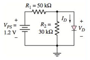
Figure P1.40
Expert Solution & Answer
Want to see the full answer?
Check out a sample textbook solution
Students have asked these similar questions
(c)
Reverse recovery is a common problem in a diode. It can increase switching losses,
increase forward voltage and induce voltage surge.
(i)
Explain how reverse recovery can increase switching losses in a diode.
(ii)
Figure Q1(c) shows that characteristic of reverse recovery in a diode. Based on
the figure, calculate the peak reverse recovery current I,
I (A)
dls
dt
30 A
Q,,
1 us
3 us
Figure Q1(c): The characteristic of reverse recovery in a diode
A- If V, is a sinusoidal voltage with Vm = 40 V, and V= 15 V. Plot the waveform of the output
voltage in each of the following clippers circuits assuming ideal diodes.
B- Repeat part (A) if the diodes are silicon diodes.
R
R
R
(a)
(b)
(c)
(d)
1. Determine Vpout for the circuit in below and draw Vauts assume the diode is the
silicon type.
10 k
+10 V--
V. ov
R,
100 k
IN914
-10 V-
2. What is the output voltage that you would expect to observe across R, circuit
of Figure below? Assume that RC is large enough to prevent significant
capacitor discharge.
+24 V
10 uF
RL
10 kn
V. ov.
IN914
-24 V
Chapter 1 Solutions
Microelectronics: Circuit Analysis and Design
Ch. 1 - Calculate the intrinsic carrier concentration in...Ch. 1 - (a) Calculate the majority and minority carrier...Ch. 1 - Consider ntype GaAs at T=300K doped to a...Ch. 1 - Consider silicon at T=300K . Assume the hole...Ch. 1 - Determine the intrinsic carrier concentration in...Ch. 1 - (a) Consider silicon at T=300K . Assume that...Ch. 1 - Using the results of TYU1.2, determine the drift...Ch. 1 - The electron and hole diffusion coefficients in...Ch. 1 - A sample of silicon at T=300K is doped to...Ch. 1 - (a) Calculate Vbi for a GaAs pn junction at T=300K...
Ch. 1 - A silicon pn junction at T=300K is doped at...Ch. 1 - (a) A silicon pn junction at T=300K has a...Ch. 1 - (a) Determine Vbi for a silicon pn junction at...Ch. 1 - A silicon pn junction diode at T=300K has a...Ch. 1 - Recall that the forwardbias diode voltage...Ch. 1 - Consider the circuit in Figure 1.28. Let VPS=4V ,...Ch. 1 - (a) Consider the circuit shown in Figure 1.28. Let...Ch. 1 - The resistor parameter in the circuit shown in...Ch. 1 - Consider the diode and circuit in Exercise EX 1.8....Ch. 1 - Consider the circuit in Figure 1.28. Let R=4k and...Ch. 1 - The power supply (input) voltage in the circuit of...Ch. 1 - (a) The circuit and diode parameters for the...Ch. 1 - Determine the diffusion conductance of a pn...Ch. 1 - Determine the smallsignal diffusion resistance of...Ch. 1 - The diffusion resistance of a pn junction diode at...Ch. 1 - A pn junction diode and a Schottky diode both have...Ch. 1 - Consider the circuit shown in Figure 1.45....Ch. 1 - Consider the circuit shown in Figure 1.46. The...Ch. 1 - A Zener diode has an equivalent series resistance...Ch. 1 - The resistor in the circuit shown in Figure 1.45...Ch. 1 - Describe an intrinsic semiconductor material. What...Ch. 1 - Describe the concept of an electron and a hole as...Ch. 1 - Describe an extrinsic semiconductor material. What...Ch. 1 - Describe the concepts of drift current and...Ch. 1 - How is a pn junction formed? What is meant by a...Ch. 1 - How is a junction capacitance created in a...Ch. 1 - Write the ideal diode currentvoltage relationship....Ch. 1 - Describe the iteration method of analysis and when...Ch. 1 - Describe the piecewise linear model of a diode and...Ch. 1 - Define a load line in a simple diode circuit.Ch. 1 - Under what conditions is the smallsignal model of...Ch. 1 - Describe the operation of a simple solar cell...Ch. 1 - How do the i characteristics of a Schottky barrier...Ch. 1 - What characteristic of a Zener diode is used in...Ch. 1 - Describe the characteristics of a photodiode and a...Ch. 1 - (a) Calculate the intrinsic carrier concentration...Ch. 1 - (a) The intrinsic carrier concentration in silicon...Ch. 1 - Calculate the intrinsic carrier concentration in...Ch. 1 - (a) Find the concentration of electrons and holes...Ch. 1 - Gallium arsenide is doped with acceptor impurity...Ch. 1 - Silicon is doped with 51016 arsenic atoms/cm3 ....Ch. 1 - (a) Calculate the concentration of electrons and...Ch. 1 - A silicon sample is fabricated such that the hole...Ch. 1 - The electron concentration in silicon at T=300K is...Ch. 1 - (a) A silicon semiconductor material is to be...Ch. 1 - (a) The applied electric field in ptype silicon is...Ch. 1 - A drift current density of 120A/cm2 is established...Ch. 1 - An ntype silicon material has a resistivity of...Ch. 1 - (a) The applied conductivity of a silicon material...Ch. 1 - In GaAs, the mobilities are n=8500cm2/Vs and...Ch. 1 - The electron and hole concentrations in a sample...Ch. 1 - The hole concentration in silicon is given by...Ch. 1 - GaAs is doped to Na=1017cm3 . (a) Calculate no and...Ch. 1 - (a) Determine the builtin potential barrier Vbi in...Ch. 1 - Consider a silicon pn junction. The nregion is...Ch. 1 - The donor concentration in the nregion of a...Ch. 1 - Consider a uniformly doped GaAs pn junction with...Ch. 1 - The zerobiased junction capacitance of a silicon...Ch. 1 - The zerobias capacitance of a silicon pn junction...Ch. 1 - The doping concentrations in a silicon pn junction...Ch. 1 - (a) At what reversebias voltage does the...Ch. 1 - (a) The reversesaturation current of a pn junction...Ch. 1 - (a) The reversesaturation current of a pn junction...Ch. 1 - A silicon pn junction diode has an emission...Ch. 1 - Plot log10ID versus VD over the range 0.1VD0.7V...Ch. 1 - (a) Consider a silicon pn junction diode operating...Ch. 1 - A pn junction diode has IS=2nA . (a) Determine the...Ch. 1 - The reversebias saturation current for a set of...Ch. 1 - A germanium pn junction has a diode current of...Ch. 1 - (a)The reversesaturation current of a gallium...Ch. 1 - The reversesaturation current of a silicon pn...Ch. 1 - A silicon pn junction diode has an applied...Ch. 1 - A pn junction diode is in series with a 1M...Ch. 1 - Consider the diode circuit shown in Figure P1.39....Ch. 1 - The diode in the circuit shown in Figure P1.40 has...Ch. 1 - Prob. 1.41PCh. 1 - (a) The reversesaturation current of each diode in...Ch. 1 - (a) Consider the circuit shown in Figure P1.40....Ch. 1 - Consider the circuit shown in Figure P1.44....Ch. 1 - The cutin voltage of the diode shown in the...Ch. 1 - Find I and VO in each circuit shown in Figure...Ch. 1 - Repeat Problem 1.47 if the reversesaturation...Ch. 1 - (a) In the circuit Shown in Figure P1.49, find the...Ch. 1 - Assume each diode in the circuit shown in Figure...Ch. 1 - (a) Consider a pn junction diode biased at IDQ=1mA...Ch. 1 - Determine the smallsignal diffusion resistancefor...Ch. 1 - The diode in the circuit shown in Figure P1.53 is...Ch. 1 - The forwardbias currents in a pn junction diode...Ch. 1 - A pn junction diode and a Schottky diode have...Ch. 1 - The reversesaturation currents of a Schottky diode...Ch. 1 - Consider the Zener diode circuit shown in Figure...Ch. 1 - (a) The Zener diode in Figure P1.57 is ideal with...Ch. 1 - Consider the Zener diode circuit shown in Figure...Ch. 1 - The Output current of a pn junction diode used as...Ch. 1 - Using the currentvoltage characteristics of the...Ch. 1 - (a) Using the currentvoltage characteristics of...Ch. 1 - Use a computer simulation to generate the ideal...Ch. 1 - Use a computer simulation to find the diode...Ch. 1 - Design a diode circuit to produce the load line...Ch. 1 - Design a circuit to produce the characteristics...Ch. 1 - Design a circuit to produce the characteristics...Ch. 1 - Design a circuit to produce the characteristics...
Knowledge Booster


Learn more about
Need a deep-dive on the concept behind this application? Look no further. Learn more about this topic, electrical-engineering and related others by exploring similar questions and additional content below.Similar questions
- How is a solid-state diode tested? Explain.arrow_forwardDiodes and rectifiers allow current to _________. flow in one direction only flow in both directions divide paths of flow none of the abovearrow_forwardPower supply circuit is delivering 0.5 A and an average voltage 20 V to the load as shown in the circuit below. The ripple voltage of the half wave rectifier is 0.5 V and the diode is represented using constant voltage model. The smoothing capacitor value is equal to c 20:5A L VI-DC20V 220V omsh T 0.01 F 0.02 F 0.0167 F None of the above euerarrow_forward
- 1. Consider the following circuit, and assume all diodes are ideal. Draw the output to for a triangular input that is given below. ~ Vin R 5 KQ www V1 5V ww D1 R1 5 ΚΩ Vin 10 f -10 D2 ww V2 5V R2 5 KQ Voarrow_forwardDraw vx and v0 according to the input voltages in the circuit shown in the figure. note = R1 = 10Kohm R2 = 1kohm R3 = 1Kohm, the threshold voltages of diodes will be VE = 0.7V.arrow_forward+5 V R₁ = 5 kn VA D₁ D₂ = IDI R, = 5 kΩ Ip2 ID3 D3 VB R3 = 5 k -10 V -5 V Determine VÀ in the multi-diode circuit shown in the figure. Let VD(ON) = 0.7 V for each diode.arrow_forward
- Power supply circuit is delivering 0.5 A and an average voltage 20 V to the load as shown in the circuit below. The ripple voltage of the half wave rectifier is 0.5 V and the diode is represented using constant voltage model. The smoothing capacitor value is equal to IL-DC =0:5A RL VL-DC =20V 220V omsb O 001 F O 0.02 F O 0.0167F O None of the above Activatearrow_forwardExercises: Determine VO and Ifor each circuit in figures. Assume that each of the diode in these circuits has a forward voltage drop of 0.7 V. V₁. D 1.1.2 D V. $5.140 1.V₁=V₁=OV. 2.V₁ =V₁=SV, and 3.V=OV & V, -5V. (d) C C ΣΙΩ T-15V D₂ +201 20 V₂ 14.02 I-15V 1. No pulses at either A or B. 2.A 30 V positive pulse at A or B, and 3. Positive pulses (30 V) at both A and B. (e)arrow_forwardFind the current through the diode in the circuit shown. Assume the diode to be ideal. A 50 92 www R₁ V = 10 V O 185 mA O 46 mA O 140 mA O 28 MA 502 R₂ B Darrow_forward
- Find the current through the diode in the circuit shown in Figure. Assume the diode to be ideal. 50 Ω A R1 V = 10 V 503R D B (i) 0,5A O 0.27A O 0,2A 0.38A O 100 wwwwarrow_forwardfor the circuit shown in the figure, plot the output voltage waveform and present the resolution in sections considering that the diodes are silicon. D4 23 100k D6 100k 24 DIODE SV Vs4 [v] 20 Vo -20arrow_forward5V 3000 1000 . 2m 1 Si 4000 500 12V The circuit shown in Figure 1 contains a Si diode with a diode resistance on 1000. Use the piecewise linear model to solve the circuit. • How many nodes are in the circuit? • Determine the Thevenin voltage across the diode. Replace the diode with the appropriate model and then solve the circuit to determine the power dissipated by each resistor and the diode.arrow_forward
arrow_back_ios
SEE MORE QUESTIONS
arrow_forward_ios
Recommended textbooks for you
 Electricity for Refrigeration, Heating, and Air C...Mechanical EngineeringISBN:9781337399128Author:Russell E. SmithPublisher:Cengage Learning
Electricity for Refrigeration, Heating, and Air C...
Mechanical Engineering
ISBN:9781337399128
Author:Russell E. Smith
Publisher:Cengage Learning
Diodes Explained - The basics how diodes work working principle pn junction; Author: The Engineering Mindset;https://www.youtube.com/watch?v=Fwj_d3uO5g8;License: Standard Youtube License