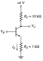
The current gain of the transistor in the circuit shown in Figure P5.32 is β = 150 . Determine I C , I E , and V C . for (a) V B = 0.2 V , (b) V B = 0.9 V , (c) V B = 1.5 V , and (d) V B = 2.2 V . Figure P5.32
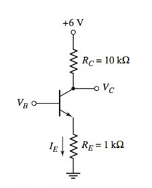
The current gain of the transistor in the circuit shown in Figure P5.32 is β = 150 . Determine I C , I E , and V C . for (a) V B = 0.2 V , (b) V B = 0.9 V , (c) V B = 1.5 V , and (d) V B = 2.2 V . Figure P5.32
The current gain of the transistor in the circuit shown in Figure P5.32 is
β
=
150
. Determine
I
C
,
I
E
, and
V
C
. for (a)
V
B
=
0.2
V
, (b)
V
B
=
0.9
V
, (c)
V
B
=
1.5
V
, and (d)
V
B
=
2.2
V
.
Figure P5.32
(a).
Expert Solution
To determine
The values of IC,IE,VC for the given circuit.
Answer to Problem 5.32P
VC=6VIC=0IE=0
Explanation of Solution
Given Information:
β=150VB=0.2V
Calculation:
Assuming the NPN transistor operates in cutoff region.
The value of VBE is:
VBE=VB−VE=0.2−0=0.2VVBE<0.7V
Hence, the assumption is correct, and transistor operates in cutoff region.
IC=0IE=0
The value of collector voltage is:
VC=6−ICRC=6−0×RC=6V
(b).
Expert Solution
To determine
The values of IC,IE,VC for the given circuit.
Answer to Problem 5.32P
IC=0.199mAIE=0.2mAVC=4V
Explanation of Solution
Given Information:
β=150VB=0.9V
Calculation:
The value of emitter current is:
Applying Kirchhoff’s voltage law in base-emitter loop:
−VB+VBE+IERE=0−0.9+0.7+IE(1k)=0IE=0.2mA
The value of collector current is:
IC=(β1+β)IEIC=(150151)×0.2mAIC=0.199mA
The value of collector voltage is:
VC=6−ICRC=6−(0.199)(10k)=4V
(c).
Expert Solution
To determine
The values of IC,IE,VC for the given circuit.
Answer to Problem 5.32P
IC=0.5mAIE=0.8mAVC=1V
Explanation of Solution
Given Information:
β=150VB=1.5V
Calculation:
The value of emitter current is:
−VB+VBE+IERE=0−1.5+0.7+IE(1k)=0IE=0.81kIE=0.8mA
The value of collector current is:
IC=(β1+β)0.8mAIC=(150151)×0.8mAIC=0.795mA
The value of collector voltage is:
VC=6−ICRC=6−(0.795mA)(10k)=−1.95V
The value of VCB is:
VCB=VC−VB=−1.95−1.5=−3.45V
The value of VCB is negative, so it is forward biased (NPN transistor). When collector base junction is forward biased then transistor operates in saturation region.
Hence, the transistor operates in saturation region.
VCE(sat)=0.2V
The emitter current is:
−VB+VBE+IERE=0−1.5+0.7+IE(1k)=0IE=0.81kIE=0.8mA
The collector current is:
Applying Kirchhoff’s voltage law in collector-emitter loop:
The value of VCB is negative, so it is forward biased (NPN transistor). When collector base junction is forward biased then transistor operates in saturation region.
Hence, the transistor operates in saturation region.
VCE(sat)=0.2V
The emitter current is:
−VB+VBE+IERE=0−2.2+0.7+IE(1k)=0IE=1.51kIE=1.5mA
The collector current is:
Applying Kirchhoff’s voltage law in collector-emitter loop:
5.47 The current gain for the transistor in the circuit in Figure P5.47 is B = 60.
Determine Rg such that Vo = 8.8 V when V, = 5 V and Ic/Ig = 25.
Vec-3v
v*-9 V
V, ww
toro
Re= 500 a
Van
LOV
Figure PS.47
Figure PS.48
5- a-) Define the MOSFET in the figure, explain by drawing its input and output circuit characteristics.b-) Since k=0.1 mA/V2, VGS=5V and VT=2.5V for this MOSFET, find the VDS voltage using the circuit.
QUESTION 4
In this voltage divider bias circuit, the input is at the base. Output is at the emitter
with a high input resistance and low output resistance. The maximum voltage gain
is 1 and the coupling capacitors must have a negligible reactance at the frequency
of operation. (use to answer a and b)
a. Derive the expression for the voltage gain, current gain, and power gain in
terms of power delivered to the load, RL.
b. Sketch both the DC and AC equivalent circuits.
c. Derive the expression for ripple factor of Half Wave Rectification with a
capacitor filter.
Need a deep-dive on the concept behind this application? Look no further. Learn more about this topic, electrical-engineering and related others by exploring similar questions and additional content below.


 Introductory Circuit Analysis (13th Edition)Electrical EngineeringISBN:9780133923605Author:Robert L. BoylestadPublisher:PEARSON
 Delmar's Standard Textbook Of ElectricityElectrical EngineeringISBN:9781337900348Author:Stephen L. HermanPublisher:Cengage Learning
 Programmable Logic ControllersElectrical EngineeringISBN:9780073373843Author:Frank D. PetruzellaPublisher:McGraw-Hill Education
 Fundamentals of Electric CircuitsElectrical EngineeringISBN:9780078028229Author:Charles K Alexander, Matthew SadikuPublisher:McGraw-Hill Education
 Electric Circuits. (11th Edition)Electrical EngineeringISBN:9780134746968Author:James W. Nilsson, Susan RiedelPublisher:PEARSON
 Engineering ElectromagneticsElectrical EngineeringISBN:9780078028151Author:Hayt, William H. (william Hart), Jr, BUCK, John A.Publisher:Mcgraw-hill Education,