Concept explainers
(a)
Find current through
(a)
Answer to Problem 59E
The current through
Explanation of Solution
Given data:
Value of trans-conductance
Value of voltage supply
Calculation:
The redrawn circuit is shown in Figure 1.
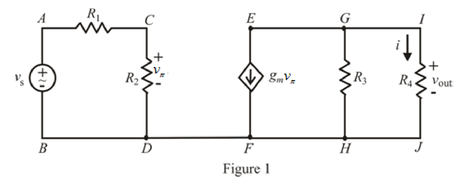
Refer to the Figure 1.
The expression for voltage division across resistance
Here,
The expression for current division rule across resistance
Here,
Substitute
Solve for
Substitute
Solve for
Conclusion:
Thus, the current across the
(b)
Find the amplifier output voltage
(b)
Answer to Problem 59E
The amplifier output voltage
Explanation of Solution
Calculation:
Refer to the Figure 1.
The expression for ohm’s law across resistance
Here,
Refer to the Figure 1.
Substitute
Conclusion:
Thus, the amplifier output voltage in the circuit is
(c)
Check whether the circuit can amplify the signal.
(c)
Answer to Problem 59E
The amplified output voltage can’t amplify the input signal because
Explanation of Solution
Refer to Figure 1
The amplified output voltage
For the amplification, the desired condition must satisfy which is
Conclusion:
Thus, the amplified output voltage can’t amplify the input signal because
(d)
Check whether the circuit can amplify the signal for input voltage
(d)
Answer to Problem 59E
The circuit can amplify the input signal because it satisfies the condition
Explanation of Solution
Refer to Figure 1
The amplified output voltage
For the amplification, the desired condition must satisfy which is
Conclusion:
Thus, circuit can amplify the input signal because it satisfies the condition
Want to see more full solutions like this?
Chapter 3 Solutions
Loose Leaf for Engineering Circuit Analysis Format: Loose-leaf


- Figure Q. 3(b) shows an op amp circuit for linear amplifier application. (i) Determine the value of current I3.(ii) Find the value of R if the output current, Io is given as 2 mA.(iii) Explain what will happen to output voltages, V01 and V02 if the supplyvoltages, +VCC and -VCC are connected to +10V and -10V.arrow_forwardSubject: Fundamentals of circuit analysis Please show all the works. The hints and answers are also given.arrow_forwardQuestion 3a) The Junction Gate Field Effect Transistor is one of the simplest types of field-effect transistor. It is a three-terminal semiconductor device .One of its function is, it serve as an amplifier. As an Engineer you are to design a single stage JFET Amplifier. Explain in your own words this circuit operates, identifyingarrow_forward
- 7) The circuit shown below is used to drive an LED with a voltage source. The circuit can also be thought of as a current amplifier in that, with the proper design, ip > i₁. (a) Derive the expression for ip in terms of i₁ and the resistors. (b) Design the circuit such that ip = 12 mA and i₁ = 1 mA for v₁ = 5 V. RE 210 R₁ www + R₂ Mli iD 7 Light OVOarrow_forwardQ3 (a) With the help of an appropriate illustration, define signal conditioning’ in the context of instrumentation and process control engineering.arrow_forwardWhat output voltage results in the circuit below for an input of 0.5 V. Refer to the following for the values of Rf = 413981 ohms, R1 = 16788 ohms. Express your answer up to two decimal places. ... V. 360 kQ 12 ko Round your answer to 2 decimal places.arrow_forward
- Design an amplifier which will produce the average of 8V, 2V and 12 V in an inverted phase. Only one amplifier is allowed to be used. i) Select the resistances accordingly and draw the circuit designing with the mentioned specifications. ii) Explain and show all calculations.arrow_forward1.a. What circuit is shown on the image above? 1.b. What is the gain? 1.c. If R2 is 40x higher than R1 what will happen to node 2? Provide waveform and explain why it happens. 1.d. Modify the circuit to have an overall gain of 2. Provide photos.arrow_forwardQ1) find for given circuit below. 1.a. What circuit is shown on the image above and what is gain ? 1.b. If R2 is 40x higher than R1 what will happen to node 2? Provide waveform and explain why it happens. 1.c. Modify the circuit to have an overall gain of 2. Provide photosarrow_forward
- Q3) b) For the circuit shown in the Figure below, find the voltage value of VCB (between collector and base). * Rc 180 N RB + Vcc 15 V 3.9 kN Bpc =100 + VBB 5 Varrow_forwardFigure Q3b shows the combination of operational amplifier circuit. Determine the: i) configuration of each op-amp, A1, A2, A3 and A4. i) output voltage, Vo. 22k Vn (V) 1uF 10k 15k +2 A, 2k2 t (ms) 2 A3 2k0 A4 OVo 0.1uF V12 (V) 2k2 +2 VizoW 10k A2 t (ms) Figure Q3barrow_forward4-) Using the DC (operating point) analysis of the following circuit, a) Find the operating point(s) of the terminal variables of the 3-terminal, b) Using the linear equivalent(s) of the 3-terminal, obtain all the possible small-signal equivalent circuits. c) Find the complete values of the voltage v2. R=3 N i iz i=v/3 i?-vi-6=0 E=6 V R3=2 2 V2 VI e(t)=0.2cos2t V E=8 Varrow_forward
 Introductory Circuit Analysis (13th Edition)Electrical EngineeringISBN:9780133923605Author:Robert L. BoylestadPublisher:PEARSON
 Delmar's Standard Textbook Of ElectricityElectrical EngineeringISBN:9781337900348Author:Stephen L. HermanPublisher:Cengage Learning
 Programmable Logic ControllersElectrical EngineeringISBN:9780073373843Author:Frank D. PetruzellaPublisher:McGraw-Hill Education
 Fundamentals of Electric CircuitsElectrical EngineeringISBN:9780078028229Author:Charles K Alexander, Matthew SadikuPublisher:McGraw-Hill Education
 Electric Circuits. (11th Edition)Electrical EngineeringISBN:9780134746968Author:James W. Nilsson, Susan RiedelPublisher:PEARSON
 Engineering ElectromagneticsElectrical EngineeringISBN:9780078028151Author:Hayt, William H. (william Hart), Jr, BUCK, John A.Publisher:Mcgraw-hill Education,