
Videos
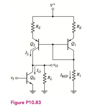
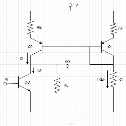
A BJT amplifier with active load is shown in Figure P10.83. The circuit contains emitter resistors
(a)
To derive:An expression for the output resistance
Answer to Problem 10.83P
Explanation of Solution
Given:
The given circuit is,

Calculation:
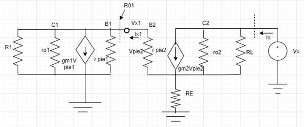
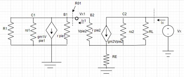
The small-signal equivalent circuit of BJT amplifier is as shown,
Apply KCL at base terminal of
Hybrid parameters p,
Substitute
Now rearrange the equation for output resistance
Expression for output resistance
Substitute equation (3) in equation (2)
Now the small-signal equivalent circuit is modified for output resistance as shown,
Apply KVL for input voltage at above circuit,
Expression for hybrid parameter.
Put
Rearrange the equation for output resistance,
Consider
Substitute the value of equation (10) in (9)
Conclusion:
(b)
To find:An expression for small-signal voltage gain.
Answer to Problem 10.83P
Explanation of Solution
Given:
The given circuit is,
Calculation:
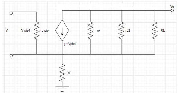
The small-signal equivalent circuit of BJT amplifier is as shown,
Apply KCL at base terminal of
Hybrid parameters p ,
Substitute
Now rearrange the equation for output resistance
Expression for output resistance
Substitute equation (3) in equation (2)
Now the small-signal equivalent circuit is modified for output resistance as shown, 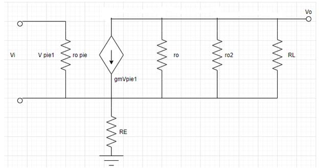
Apply KVL for input voltage at above circuit,
Expression for hybrid parameter.
Put
Rearrange the equation for output resistance,
Consider
Substitute the value of equation 10 in equation 9,
Now derive an expression for output voltage.
Input voltage will be,
Put
It is known that ,
The small-signal voltage gain derived expression is,
Conclusion:
Want to see more full solutions like this?
Chapter 10 Solutions
Microelectronics: Circuit Analysis and Design


- 2 a) i) Draw typical output characteristics of a common emitter npn transistor and clearly identify the active, saturation, and cut off regions on your drawing. ii) Explain how you can find the common emitter de current gain, B, and the common emitter ac current gain, hre, from the common emitter output characteristics of an npn transistor. You need to draw typical output characteristics in scales and provide numerical calculations to support your explanation.arrow_forwardQ.1/ Figure below shows a CE power amplifier in which the collector resistor serves also as the load resistor. Assume DC=ac=100.a. Determines the dc Q-point (ICQ and VCEQ).b. Determine the voltage gain and the power gain.c. What changes would be necessary to convert the circuit to a pnp transistor with a positive supply? What advantage would this have?arrow_forwardDiscuss the working of transistor as an amplifier alsocalculate its voltage gain.arrow_forward
- Q.2/ For the amplifier’s circuits shown below:a. Determine the Q-point for each amplifier circuit.b. What is the maximum peak value of collector current that can be realized in each circuit?c. What is the maximum peak value of output voltage in each circuit?arrow_forwardDraw the circuit symbol for a NPN BJT. Label the terminals and currents. Chose the reference directions that agree with the true current directions for operation in the amplifier region.arrow_forwardDesign a voltage divider biased CE stage with emitter degeneration. That stage should support a voltage gain of 5 and an input impedance larger than 3 KOhms with a bias current of 0.5 mA. Assume Beta=100, Is = 5e-17. Neglect the early voltage effect. You also need to provide values for the operating point of this transistor. Find the output resistance of this stage if the early voltage = 20 V.arrow_forward
- What are the advantages of active load with respect to passive load in transistors? Write down at least 5 advantages.arrow_forward34 Shown in Figure P10.34 is a common-emitter amplifier stage implemented with an npn silicon transistor. The DC bias circuit connected to the base consists of a single resistor; however, it is connected directly between base and collector. Determine VCEQ and the region of operation. Vcc = 12 V B = 130 Rg = 325 k2 Rc = 1.9 k2 Rg = 2.3 k2 R = 10 k2 Rs = 0.5 k2 vs = 1 cos(6.28 × 10°t) mV Rc Vc RE RE R1arrow_forwardConsider the MOSFET amplifer circuit shown in Figure below. Assume µnCox(W/L) = 4mA/V2, Vt = 1V Draw an equivalent DC model, and equivalent circuit of the amplifier. Determine the drain current and its overall voltage gain respectively.arrow_forward
- A Darlington pair of transistors is connected asshown in Figure P10.39. The transistor parameters forlarge-signal operation are Q1: β = 130; Q2: β = 70.Calculate the overall current gain.arrow_forward5) Design a Common source E-MOSFET amplifier and write the formula of voltage gain.arrow_forwardExplain how you can find the common emitter de current gain, B, and the common emitter ac current gain, hre, from the common emitter output characteristics of an npn transistor. You need to draw typical output characteristics in scales and provide numerical calculations to support your explanation.arrow_forward
 Introductory Circuit Analysis (13th Edition)Electrical EngineeringISBN:9780133923605Author:Robert L. BoylestadPublisher:PEARSON
 Delmar's Standard Textbook Of ElectricityElectrical EngineeringISBN:9781337900348Author:Stephen L. HermanPublisher:Cengage Learning
 Programmable Logic ControllersElectrical EngineeringISBN:9780073373843Author:Frank D. PetruzellaPublisher:McGraw-Hill Education
 Fundamentals of Electric CircuitsElectrical EngineeringISBN:9780078028229Author:Charles K Alexander, Matthew SadikuPublisher:McGraw-Hill Education
 Electric Circuits. (11th Edition)Electrical EngineeringISBN:9780134746968Author:James W. Nilsson, Susan RiedelPublisher:PEARSON
 Engineering ElectromagneticsElectrical EngineeringISBN:9780078028151Author:Hayt, William H. (william Hart), Jr, BUCK, John A.Publisher:Mcgraw-hill Education,