
Concept explainers
(a)
Thevalue of the voltage
(a)
Answer to Problem 8.26P
The value of the voltage
Explanation of Solution
Calculation:
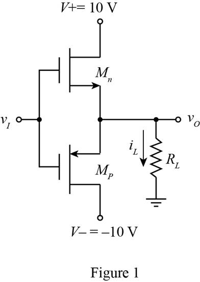
The given diagram is shown in Figure 1
The conversion from
The expression for the collector current is given by,
Substitute
The expression for the base emitter voltage of the NPN transistor for no input voltage is given by,
The expression for the base emitter voltage for the PNP transistor for zero input voltage is given by,
From the above equation and equation (1).
Substitute
The expression for the power dissipated in the transistor is given by,
Substitute
Conclusion:
Therefore, the value of the voltage
(b)
The value of the power dissipated in
(b)
Answer to Problem 8.26P
The value of
Explanation of Solution
Calculation:
The expression for the value of the load current is given by,
Substitute
The expression for the current through the PNP transistor is given by,
Substitute
The conversion from
The conversion from
The expression for the value of the base to emitter voltage of PNP transistor is given by,
Substitute
The expression to determine the value of the base emitter voltage of the NPN transistor is given by,
Substitute
The expression for the collector current of the NPN transistor is given by,
Substitute
The expression for the value of collector current of PNP transistor is given by,
Substitute
Apply KVL at the input terminals of the given figure.
Substitute
The expression for the power dissipated in the load is given by,
Substitute
The expression for the value of power dissipated in the transistor is given by,
Substitute
The expression for the power dissipated in the PNP transistor is given by,
Substitute
Conclusion:
Therefore, the value of
Want to see more full solutions like this?
Chapter 8 Solutions
Microelectronics: Circuit Analysis and Design


- Answwr for both circuit... Answer for both cktarrow_forwardDiscussion 1. Calculate the theoretical DC voltages and currents for the transistor bias circuit and compare them with the practically measured values. Table-1: Measured Quantities for the DC Bias Circuit Parameter B VB VE Vc Icọ VCEQ VBEQ Te Value 65.63 1.20 0.58 7.32 1418mA 6.74 0,62 18.3356 ECTR Vcc +12V R5 R3 3.3kQ всз37 R2 R4 4.7kQ 4700 Figure 5: The DC Bias Circuit of the Common Emitter Amplifierarrow_forwardElectrical Engineering A uniformly doped silicon pnp bipolar transistor is to be designed with NĘ = 1019 cm³ and Nc = 1016 cm³. The metallurgical base width is 0.75 µm. Determine the minimum base doping so that the punch- through voltage is no less than 25 V.arrow_forward
- b) Consider the transistor circuit as shown in figure 8. The emitter area of the transistor Q2 is 20 times the other transistors. Calculate the value of Ic, and Ic,.Assume that the ß of the transistor is very high. SmA Q1 Ic2 Q2 Figure 8arrow_forwardAssume Icq = 3mA, Vceq = 10V for the given transistor circuit. %3D Find the R1 and Rc values. 22V Rc R1 Text 10uF 10uF 20 k2 31.2 k2arrow_forwardWhen operated in cutoff and saturation, the transistor acts like a) A linear amplifier b) A switch c) A variable capacitor d) A variable resistor The average output value of half wave rectified voltage with a peak input of 200V is equal to (assume silicon diode) a) 63.66 V b) 127.32 V c) 63.47 V d) 127.101 V The term "Bipolar" in Bipolar Junction Transistor (BJT) refers to a) Two junctions b) Two Diodes c) Two polarity carriers (electrons & holes) d) Two resistancesarrow_forward
- Measurements taken with an E-MOSFET indicate that when VGS=+4V, ID=8mA, and when VGS=+6V, ID=32mA. Determine the value of k.arrow_forwardUsing the re model circuit, determine the total voltage gain for the BJT circuit shown below. Show the details of your work. 22V ... 5.6k0 330k Vo + 10UF-POL B = 80 1200 10UF-POL To = 40 kN 2N2221 6.8k) Vs 4700 22UF-POLarrow_forwardA base bias method is used in the following circuit. For Bpc - 300, the value of emitter current is: -Vc. +15 V Rc 1.8 k2 RB 560 k2 7.82 mA O 6.84 mA O 7.27 mAarrow_forward
- 1-The output voltage of an emitter follower is a-In phase with Vin . b-Much greater than Vin. c-180° out of phase. d-Generally much less than Vin • 2-The ac emitter resistance of an emitter follower a-Equal the de emitter resistance. b-Is larger than the load resistance. c-Is B times smaller than the load resistance. d-Is usually less than the load resistance. 3-A common-base amplifier can be used when a-Matching low to high impedance. b-A voltage gain without a current gain is required. c-A high- frequency amplifier is needed. d-All of the above. 4-If the voltage generator is 5 mV in an emitter follower, the output voltage across the load is closest to a-5 mV. b-150mV. c-0.25 mV. d-0.5 mV.arrow_forwardExample 7 Rc 100N Determine IB , IC , IE , VBE, VCE, and VCB in pou P Rg Vcc the circuit. The transistor has a BDC = 150. 10 V 10 kN VBB 5 Varrow_forwardConsider the circuit below. Assume IB, total=0.020mA Calculate the IC total in mA for both BJTs have the same B=100.arrow_forward
 Introductory Circuit Analysis (13th Edition)Electrical EngineeringISBN:9780133923605Author:Robert L. BoylestadPublisher:PEARSON
 Delmar's Standard Textbook Of ElectricityElectrical EngineeringISBN:9781337900348Author:Stephen L. HermanPublisher:Cengage Learning
 Programmable Logic ControllersElectrical EngineeringISBN:9780073373843Author:Frank D. PetruzellaPublisher:McGraw-Hill Education
 Fundamentals of Electric CircuitsElectrical EngineeringISBN:9780078028229Author:Charles K Alexander, Matthew SadikuPublisher:McGraw-Hill Education
 Electric Circuits. (11th Edition)Electrical EngineeringISBN:9780134746968Author:James W. Nilsson, Susan RiedelPublisher:PEARSON
 Engineering ElectromagneticsElectrical EngineeringISBN:9780078028151Author:Hayt, William H. (william Hart), Jr, BUCK, John A.Publisher:Mcgraw-hill Education,