
Concept explainers
Videos
Assume
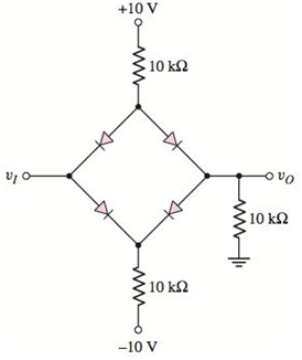
Figure P2.51
To plot: The output voltage,
Explanation of Solution
Given:
Calculation:
Case 1:
Assume that diodes
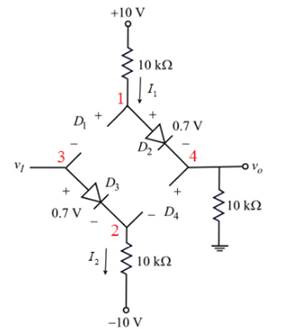
Figure 1
Apply the Kirchhoff’s voltage to the outer branch of the circuit shown in figure 1.
Therefore,
The voltage at node
The voltage at node
Apply the Kirchhoff’s voltage to the input branch of the circuit shown in figure
Therefore,
The voltage at node
The diode
The diode
Therefore, diodes
The output voltage is constant for
Case 2:
Assume that diodes
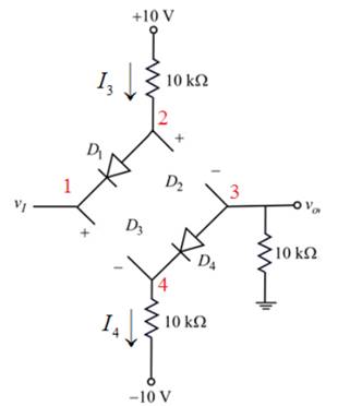
Figure 2
Apply the Kirchhoff’s voltage to the outer branch of the circuit shown in figure 2.
The voltage at node
The voltage at node
Apply the Kirchhoff’s voltage to the input branch of the circuit shown in figure 2.
Therefore,
The voltage at node
The diode
The diode
Therefore, diodes
Therefore, the output voltage is constant for
Case 3:
Assume that diodes
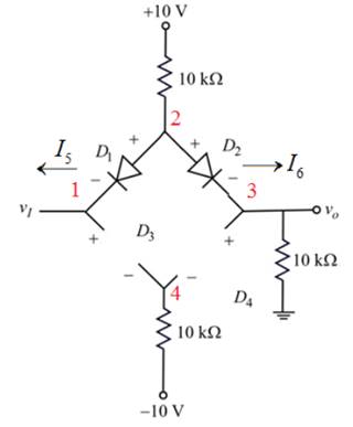
Figure 3
Apply the Kirchhoff’s current law at node
The diode
Apply the Kirchhoff’s voltage law to the input branch of the circuit shown in figure 3.
The voltage across diode
Consider equation(1).
Rewrite as,
Therefore, the output voltage is,
Therefore, plot
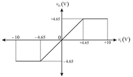
Conclusion:
Therefore, plot of
Want to see more full solutions like this?
Chapter 2 Solutions
Microelectronics: Circuit Analysis and Design


- How is a solid-state diode tested? Explain.arrow_forwardIn the circuit given in the figure, find the current passing through the diode in mA since R1 = 4.95Kohm, R2 = 2.50Kohm, R3 = 1.69Kohm, R4 = 5.44Kohm, VCC = 13.00V and the diode is silicon?arrow_forwardAssuming an ideal diode model for all the diodes in the circuit below, Calculate the voltage across and current flow through each diode R1 9k0 IN1199C 01 18k IN1199C D3 IN1199C 12 1k0 R4 SkO 1- V 11 mA 0.5 mA 0.1 A Oarrow_forward
- 120 V rms elile a. DI D2 # What is the peak current through each diode? b. What is the P/V for each diode? (Ctrl) - 5ΚΩarrow_forward0:- Consider the circuit in Figure a) What type of circuit is this? b) Find and Sketch the voltage waveform across RL, assume the diodes are practical. c) If 100uf capacitor parallel with the resistor, calculate the ripple is connected factor I O o Darrow_forwardFor the circuit below, assume the diodes operate with a constant voltage drop of .7V, find Vx, Vy, VD4 and ID2. 15V 15V Allt V1 V2 R1 1k IDC 1mA Vx R2 2k ww D1N4002 Vy D1N4002 7D1 D1N4002 D2 D3 R3 1k D4 D1N4002arrow_forward
- 1. Determine Vpout for the circuit in below and draw Vauts assume the diode is the silicon type. 10 k +10 V-- V. ov R, 100 k IN914 -10 V- 2. What is the output voltage that you would expect to observe across R, circuit of Figure below? Assume that RC is large enough to prevent significant capacitor discharge. +24 V 10 uF RL 10 kn V. ov. IN914 -24 Varrow_forwardDraw vx and v0 according to the input voltages in the circuit shown in the figure. note = R1 = 10Kohm R2 = 1kohm R3 = 1Kohm, the threshold voltages of diodes will be VE = 0.7V.arrow_forwardAssuming an ideal diode model for all the diodes in the circuit below, Calculate the voltage across and current flow through each diode R1 D2 9kQ 1N1199C R2 D1 18k0 1N1199C V2 12 V R3 1kQ D3 1N1199C R4 5k0arrow_forward
- Draw output waveform for the following circuit. Suppose input is a pure square wave with a positive half at 10 V and negative half at -10 V for ideal diodes. D1 D2 220 R3 R1 1k R2 1karrow_forwardDetermine the negative resistance for the tunnel diode in the figure between ?T = 0.2 ? and ?T = 0.4arrow_forwardSince R1=4.51 Kohm, R2=1.19 Kohm R3=2.74Kohm R4=5.60Kohm VCC=23.00V and diode silicon in the circuit given in the figure, find the current passing through the diode in mAarrow_forward
