
a.
The differential-mode voltage gain
a.
Answer to Problem 11.92P
Explanation of Solution
Given:
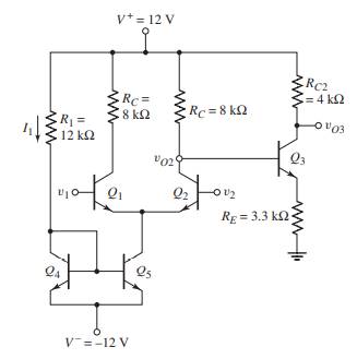
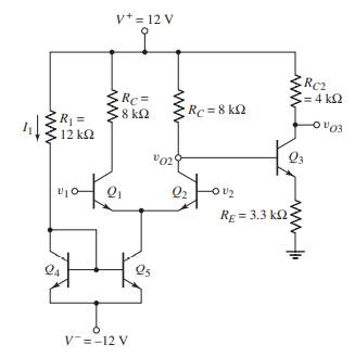
The given circuit is,
Calculation:
Consider the given figure,
The voltage
The input resistance of the CE amplifier is,
Now calculate the output resistance,
Now calculate
Hence,
b.
The output voltage
To compare: The obtained result with the ideal output.
b.
Answer to Problem 11.92P
The output voltage obtained for ideal case is greater than the actual result obtained.
Explanation of Solution
Given:
The given circuit is,
Calculation:
Consider the given voltage,
The differential input voltage will be,
Now calculate output voltage,
Now calculate output voltage for ideal case,
Put
Hence,
It is observed that both the values are slightly different. The output voltage obtained for ideal case is greater than the actual result obtained.
c.
The differential-mode and common-mode input resistances.
c.
Answer to Problem 11.92P
Explanation of Solution
Given:
The given circuit is,

Calculation:
Let calculatethe differential-mode input resistances,
The common-mode input resistances will be,
Hence,
Want to see more full solutions like this?
Chapter 11 Solutions
Microelectronics: Circuit Analysis and Design

- Determine the DC bias values using DC equivalent circuits (in order of VE, VB, VC)arrow_forwardClass B Amplifier q1)If the input is 7.5Vp-p...DATA COLLECTION: What is the IL(peak)? a)7mA 6)mA 5)mA 4)mA q2) DATA COLLECTION: What is the Idc? a)3.84 b)4.82 c)3.82mA d)1.82mA q3)DATA COLLECTION: What is the input power in DC? Power input = 48.45mW Power input = 45.48mW Power input = 44.58mW Power input = 45.84mW q4) DATA COLLECTION: What is the output power in AC? a)18mW b)81mW c)11.8mW d)18.9mW q5)DATA COLLECTION: What is the power dissapated by each transistor? a)35.1mW b)53.1mW c)15.3mW d)13.5mW q6)DATA COLLECTION: What is the efficiency of class B amplifier? a)45% b)40% c)63% d)33% q7)arrow_forward........ (Figure-1) R. RB= 380kN,Rc= 1kN B = 100, VBB = Vcc=12V RB ww Vec CC ......... I, V CE СЕ V ВЕ BB Q-1-b) Describe briefly the input / output characteristics and application of Common Emitter BJT Configurationarrow_forward
- Sketch the de load line, quiescent collector current, quiescent voltsge, input power, output power and maximum efficiency of the circuit shown an Figure. The input results in a base current of 5 mA peak to peak What maximum output power can be delivered by the circuit, if the input voltage is changed resulting in a base current of 10mA peak to peak and hence find the maximum etficiency. cc=15 V R =18 2 -25arrow_forwardCalculate the output impedance for small-signal equivalent circuit. (R1=10 k ohm, r0, =10 k ohm)arrow_forwardA. Detemine the value of the collector resistor in an npn transistor amplifier with Bpc = 250, VBB = 2.5 V, Vcc = 9 V, VCE = 4 V, and Rg = 100 k2. B. Detemine Ic(sat) for the transistor in below Figure. What is the value of Is necessary to produce saturation? What minimum value of VIN is necessary for saturation? Assume VCE(sat) = 0 V. %3D +5 V 10 kN Rg VINO BDC = 150 1.0 MNarrow_forward
- A) Design with drawing an Op-Amp series voltage regulator to give a regulated O/P voltage of 12V for an I/P of 15V B) Calculate the line regulation if the I/p increases to 4V leads to increase the O/P voltage to 0.02V.arrow_forward1. Without bypass capacitor CE, determine Av2. Without bypass capacitor CE, determine the current gainarrow_forwardWhy there is a difference between the value of a beta dc and the value of a beta ac in the diagram of output characteristics in transistorarrow_forward
- Calculate the closed loop gain for the following circuit. Assume A = 0 for both transistors and R1+ R2 is very large. Circuit parameters / Devre Parametreleri 9m1 = 49 ms, 9m2 = 33 ms, R, = 101 kn, R2 = 26 k, Rp = 2.2 kn VDD Rp Vout ER Vino ER2 O a. 10.28 O b. 4.67 O c. 8.41 O d. 7.48 O e. 6.54 O f. 3.74 O g. 5.61 O h. 2.80 W WH. w-arrow_forwardc. For the circuit shown in Figure, determine lc and VCB. Assume the transistor to be made of Silicon. Ic RE=1.6 kn Rc=1.1 kn EE=8 V Vcc= 20 varrow_forward11. i) Design a series Op-Amp regulated O/P of 12V which its I/P voltage is 20V. Chose the designed components and draw the circuit diagram ii) Design a shunt transistor regulated O/P of 6V which its I/P voltage is 15V. Chose the designed components and calculate I, with drawing the circuit diagramarrow_forward
 Introductory Circuit Analysis (13th Edition)Electrical EngineeringISBN:9780133923605Author:Robert L. BoylestadPublisher:PEARSON
 Delmar's Standard Textbook Of ElectricityElectrical EngineeringISBN:9781337900348Author:Stephen L. HermanPublisher:Cengage Learning
 Programmable Logic ControllersElectrical EngineeringISBN:9780073373843Author:Frank D. PetruzellaPublisher:McGraw-Hill Education
 Fundamentals of Electric CircuitsElectrical EngineeringISBN:9780078028229Author:Charles K Alexander, Matthew SadikuPublisher:McGraw-Hill Education
 Electric Circuits. (11th Edition)Electrical EngineeringISBN:9780134746968Author:James W. Nilsson, Susan RiedelPublisher:PEARSON
 Engineering ElectromagneticsElectrical EngineeringISBN:9780078028151Author:Hayt, William H. (william Hart), Jr, BUCK, John A.Publisher:Mcgraw-hill Education,