
Concept explainers
The value of
Answer to Problem 10.60P
Explanation of Solution
Given:
Calculation:
The given circuit is,
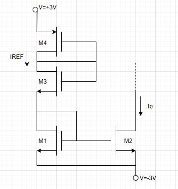
Current through transistors
Consider equation (2)
Now on considering equation (3),
From the circuit,
On substituting the given value,
Substitute
Substitute
Now calculate
Hence
Now calculate
Conclusion:
Want to see more full solutions like this?
Chapter 10 Solutions
Microelectronics: Circuit Analysis and Design


- Q1. The output characteristic of a typical transistor is shown below, where the quiescent point is selected on it. This transistor is used in the bias circuit presented below. Find the suitable values of Rg and Rc to fix the Q-point of the circuit properly. +Vcc = 12 V 12- Is = 70 uA 10- Ig = 60 uA 8- Rc Is = 50 uA Rs 6- Ig= 40 uA 4. Is = 30 uĄ Is = 20 uA B = 100 2- VBE = 0.7 V 0- -2- 2 4 6 8 10 12 14 16 VCE (V) Ic (mA)arrow_forward31 The circuit shown in Figure P10.31 is a common-emitter amplifier stage. Determine the Thévenin equivalent of the part of the circuit containing R1, R2, and Væ with respect to the terminals of R2. Redraw the schematic, using the Thévenin equivalent. Vcc = 20 V B = 130 R = 1.8 M2 R2 = 300 k2 %3D Rc = 3 k2 Rg = 1 k2 %3D %3D R = 1 k2 Rs = 0.6 k2 vs = 1 cos(6.28 x 10³t) mV Rc R1 Vcc R1EV. RS R2 V's Vị REarrow_forward5V B OV OV For all the MOSFETS assume Vth=1V and k =50 mA/V² R₁ = 4700 Ao M₁ M₂ B Indicate and verify the state of each MOSFET and Vo for the following input combinations. Fill out the table for each assumed state of the MOSFET for every input combination. Use Rds(on) approximation for linear operation and three significant figures for the voltages. M1 is assumed to be in saturation. If Vgs = 2 V, Vds = 4V, Vds > Vgs - Vth 4>2-1 4> 1 (ok) Vgs > Vth (2>1) A M2 state M3 state V. 0 OV 5 V R₂ = 560Ω 5V M1 state M3arrow_forward
- Design counter 0,2,4,6,… with JKFF and DFFarrow_forwardReferring to Figure 2 and the following BJT parameters: ß = 100, thermal voltage = 25 mV and VBE = 0.7 V. a. Calculate the DC operating point of the BJT which are the collector current, Ic and base-emitter voltage, VCE. b. Draw the low-frequency small-signal equivalent circuit for Figure 2. c. If v = (Mx10-8)sin(wt) V where M is your matric number, calculate the instantaneous positive peak collector voltage, Ve(peak). d. Explain the effect of CE on the BJT DC operating point and the small- signal voltage gain. Vc 10V Rc $4.7 ka R1 47 ko3 B=100 Vthermai=25mv R2 10 kn3 CE |10uf RE $1ko GND Figure 2arrow_forward2) Consider the circuit given below. (Assume: K-4mA/V', Vt=-1V, A=0, (K= µCox.(W/L)) da Perform DC analysis and calculate Va. Vsg, Vs, voltages, and Ip, gm, ro values bo Draw a small-signal equivalent circuit Co Calculate Av, Rin, Rout values as shown on the schematic Also ) satwaton mode Test for Fill inthe table VG VSG O2m A Rin Vs QUin ID vo Coo 9m Ro Av Rout Rin Routarrow_forward
- Using LTSpice, simulate the circuit below, use 2N3904 for the transistor. Part ! DC simulation: Measure VCE and Ic. Use .op for the simulation cmd. Remove all capacitors and input signals first. Part 2 AC simulation: Connect all capacitors now and apply an AC signal at the input with an amplitufe of 1mV and a frequency of 1kHz. Determine the Voltage gain of the circuit by dividing Vo with Vin. Show the output for both the DC and AC analysis. Take a screenshot of the circuit and the output voltages and waveforms. Paste in a word file, write your answers, then save as pdf. 50 kΩ Σ 20 0,5 ΚΩ wwwh 9 Vcc=20 V Ca=1 µF = Cc₂ Cg=50 μF 5.6 kn B=100 Ca IST • 3.3 ΚΩ 5 ΚΩΣ CEarrow_forward34 Shown in Figure P10.34 is a common-emitter amplifier stage implemented with an npn silicon transistor. The DC bias circuit connected to the base consists of a single resistor; however, it is connected directly between base and collector. Determine VCEQ and the region of operation. Vcc = 12 V B = 130 Rg = 325 k2 Rc = 1.9 k2 Rg = 2.3 k2 R = 10 k2 Rs = 0.5 k2 vs = 1 cos(6.28 × 10°t) mV Rc Vc RE RE R1arrow_forward........ (Figure-1) R. RB= 380kN,Rc= 1kN B = 100, VBB = Vcc=12V RB ww Vec CC ......... I, V CE СЕ V ВЕ BB Q-1-b) Describe briefly the input / output characteristics and application of Common Emitter BJT Configurationarrow_forward
- An emitter follower output stage has Vcc = 10 V, R3 =5 k2, VCEsat= 0.2 V, RL = 1 kQ. Assume the signals are sinusoidal. +Vec A) select R1 and R2 to make the efficiency 10% Hint: IQ must be more than IR B) If R1=R2=0. select R3 to make RL follow the situation of RL1. calculate the corresponding load power , efficiency, and the maximum instantaneous power dissipation in Q1 -Vec 21arrow_forward5, a) Determine Vdsat when ID=.5 mA. b) Determine Kn when ID = 0.5 Amps. (Show your work!) c) Determine VTN. (Show your work!) d) Vgs Consider the circuit and corresponding graph, shown below. ID (mA) 0.60 0.50 0.40 0.30 0.20 0.10 0.00 0 0.5 Vds 1 1.5 2 2.5 Vds 3 3.5 4 4.5 5 -Vgs = 1V - Vgs = 1.1V - Vgs = 1.2V - Vgs = 1.3Varrow_forwardDetermine the input resistance Rin as indicated in the figure. Ignore resistor ro of the transistor and capacitors are large. A. Rin = R1//R2//R3 B. Rin = R2//R3 (//R4//R5) C. Rin = R2//R3 // ( r π + [1+gm r π ] (//R4//R5) ) D. Rin = R2//R3 // r π (//R4//R5) )arrow_forward
 Introductory Circuit Analysis (13th Edition)Electrical EngineeringISBN:9780133923605Author:Robert L. BoylestadPublisher:PEARSON
 Delmar's Standard Textbook Of ElectricityElectrical EngineeringISBN:9781337900348Author:Stephen L. HermanPublisher:Cengage Learning
 Programmable Logic ControllersElectrical EngineeringISBN:9780073373843Author:Frank D. PetruzellaPublisher:McGraw-Hill Education
 Fundamentals of Electric CircuitsElectrical EngineeringISBN:9780078028229Author:Charles K Alexander, Matthew SadikuPublisher:McGraw-Hill Education
 Electric Circuits. (11th Edition)Electrical EngineeringISBN:9780134746968Author:James W. Nilsson, Susan RiedelPublisher:PEARSON
 Engineering ElectromagneticsElectrical EngineeringISBN:9780078028151Author:Hayt, William H. (william Hart), Jr, BUCK, John A.Publisher:Mcgraw-hill Education,