
Concept explainers
Videos
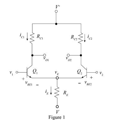
Consider the differential amplifier circuit in Figure 17.1 biased at
(a)
The design parameters of the circuit for the given values.
Answer to Problem 17.1EP
The value of the resistances to design the circuit are for
Explanation of Solution
Calculation:
The given circuit is shown in Figure 1.
The expression for the voltage at the emitter terminals is given by,
Substitute
The expression to determine the value of the current
Substitute
The expression to determine the value of the collector current of the first transistor is given by,
Substitute
The expression for the value of the collector current of the second transistor is given by,
Substitute
The expression for the value of the voltage
Substitute
Conclusion:
Therefore, the value of the resistances to design the circuit are for
(b)
The value of the current
Answer to Problem 17.1EP
The value of the current and the voltage for the value of the input voltage of
Explanation of Solution
Calculation:
The expression for the voltage at the emitter terminals is given by,
Substitute
The expression to determine the value of the current
Substitute
The expression to determine the value of the collector current of the first transistor is given by,
Substitute
The expression for the value of the collector current of the second transistor is given by,
The expression for the value of the voltage
Substitute
The expression for the value of the voltage
Substitute
The expression for the voltage at the emitter terminals is given by,
Substitute
The expression to determine the value of the current
Substitute
The expression to determine the value of the collector current of the first transistor is given by,
The expression for the value of the collector current of the second transistor is given by,
Substitute
The expression for the value of the voltage
Substitute
The expression for the value of the voltage
Substitute
Conclusion:
Therefore, the value of the current and the voltage for the value of the input voltage of
(c)
The value of the power dissipated in the circuit for the different value of the input voltage.
Answer to Problem 17.1EP
The value of the power consumed in the circuit for the input voltage of
Explanation of Solution
Calculation:
The expression for the value of the power dissipated in the circuit.
Substitute
Substitute
Conclusion:
Therefore, the value of the power consumed in the circuit for the input voltage of
Want to see more full solutions like this?
Chapter 17 Solutions
Microelectronics: Circuit Analysis and Design


- 2. The parameters of the transistor as shown in the figure below are ß = 100 and VA = 100V. a. Find the dc voltages at the base and emitter terminals. b. Find Rc such that VCEQ = 3.5V. c. Assuming Cc and CE act as short circuits, determine the small-signal voltage gain Av = Vo/Vs. d. Repeat part (c) if a 5000 source resistor is in series with the vs signal source. V+ = +5 V Rs = 100 £2 www Us Cc RB = 10 ΚΩ I= Iausmi 0.35 mA www RC -000 V=-5 V CEarrow_forwardDerive the output resistance using small signal model for the following circuits, assuming the transistor has output resistance of a transistor is ro and transconductance of gm. Rout PPA Rout Vb- Vbo Rout Rout Vdd Vb- Routarrow_forward11. An SCR bridge takes power from a 120 VRMS 60 Hz source, and provides it to a load at a nomi- nal 72 V dc. a. What phase delay angle a will be used to meet this requirement? b. Plot the output voltage of the bridge, one of the switching functions, and the input current wave- form for your value of a from part (a), given a large output inductor and a 10 A load. c. If the output power is to be 1 kW, what value of inductance will be needed to keep the output ripple below 1% peak-to-peak?arrow_forward
- Define in your own words what is a small signal FET when it comes to Av, Ai, ri, ro of the circuit.arrow_forwardInstruction/s: Draw, Illustrate and label your schematic diagram before solving the problem.2.) Given a Collector -Feedback Biased transistor circuit with voltage at common collector is +10v ,base resistor is 100k ohms, Collector resistor is 10k ohms and Base current is 8.38 micro ampere, ,Voltage at Base-emitter junction is 0.7v. Determine Beta DC , Collector current and Voltage at collector-emitter junction. These might help as a guide to answer the problem...arrow_forwardV* = + |ov Ri Rip ERC Vs RE V: -sV The following parameters are given for this transistor: B = 200 and VA = o. Design the circuit with the following value ICQ = 1.5mA and VCEQ = 5V. Find the small signal voltage gain AV = Vo/Vs. Find the input resistance in the signal source Vs.arrow_forward
- A differential amplifier has a common mode gain of 0.2 and CMMR = 80dB. The differentialmode gain is given byA) 2000 B) 10000 C) 40 D) 0arrow_forwardFill in the table VB VC VE Ic LE I8 fre IT gm 5V Consider the circuit given at the right. 600k 1.5k =0.7, Vauo, B=165) 100uF Vo 1k 100uF a) Perform DC analysis and calculate all VB =? VC:? branch currents, node voltages, and small signal parameters 3K VE=? Rout b) Draw a small-signal equivalent model n Vin Rin 400K c) Calculate Ri, Rout, and Ay=Vou/Vin -5Varrow_forwardFor an enhancement NMOSFET source follower, V-2V, k, = k,'(W/L) = 1 mA/V?, Ri- 2MΩ, R=1 MΩ, Ri-8kΩ, Rs-2kΩ Calculate Ip and VDs. (a) (b) Draw the small signal equivalent circuit and determine gm. Determine the input resistance Rin and the output resistance Ro. Determine the voltage gain Av = vo/vị and current gain Aj = i/i. V=15V R, Rह R Rn Answer: (a) Ip = Vps = (b) Equivalent circuit, gm= (c) Rin = Ro = (d) Av = v/vi = Aj = i/i =arrow_forward
- Develop the voltage transfer curves (VO versus VI) for the amplifier circuits shown (a) and (b). Assume npn transistor parameters of VBE(on) = 0.7V, ß = 120, and VCE(sat) = 0.2V, and pnp transistor parameters of VEB(on) = 0.7V, B = 80, and VEC(sat) = 0.2V. Amplifier circuits are often biased to give a maximum swing of input and output voltage. Mark this dc bias (or Q-point) on the voltage transfer curves. What is the amplification factor (or voltage gain)? v* = +5 V v* = +5 V Re = 5 k2 Ry = 200 k2 V, o ww Rg = 150 k2 V,o ww Rc = 8 k2 (a) (b)arrow_forwardFor these circuit finf the input impedanc Zi only .....arrow_forward1) Consider the circuit given below. (Assume: K=4mA/V', Vt=1V, A=0, (K= uCox.(W/L) a) Perform DC analysis and calculate Va Ves, Vs, lon gm, ro values. Fill in the table b) Draw a small-signal equivalent circuit c) Calculate Av, Ri, Ro values as shown on the schematic ID 5V R, 2Meg Vs Rsig:100k Coo Ro Co gm Vsig ' Rz $ 2Meg 2K :RL 1OK 1RO나나 Rout ro Rin Av Vo Bi Ava vsig Roarrow_forward
 Introductory Circuit Analysis (13th Edition)Electrical EngineeringISBN:9780133923605Author:Robert L. BoylestadPublisher:PEARSON
 Delmar's Standard Textbook Of ElectricityElectrical EngineeringISBN:9781337900348Author:Stephen L. HermanPublisher:Cengage Learning
 Programmable Logic ControllersElectrical EngineeringISBN:9780073373843Author:Frank D. PetruzellaPublisher:McGraw-Hill Education
 Fundamentals of Electric CircuitsElectrical EngineeringISBN:9780078028229Author:Charles K Alexander, Matthew SadikuPublisher:McGraw-Hill Education
 Electric Circuits. (11th Edition)Electrical EngineeringISBN:9780134746968Author:James W. Nilsson, Susan RiedelPublisher:PEARSON
 Engineering ElectromagneticsElectrical EngineeringISBN:9780078028151Author:Hayt, William H. (william Hart), Jr, BUCK, John A.Publisher:Mcgraw-hill Education,